Because of the holidays, TI E2E™ design support forum responses will be delayed from Dec. 25 through Jan. 2. Thank you for your patience.

This thread has been locked.

If you have a related question, please click the "Ask a related question" button in the top right corner. The newly created question will be automatically linked to this question.

UCC27511: Gate driver and mosfet is getting failed

Part Number: UCC27511

I am using UCC27511 single channel gate driver to drive 700W LED module (Output Voltage 375 to 390). We are implementing non inverting driver configuration as in application note (Fig 25 in datasheet) to drive mosfet PSM20N60CT. I am using R1 = 5.1ohm and R2= 0.5ohm as gate resistors and a gate to sourse resistor of 10K. The problem i am facing is that the gate driver and mosfet is getting failed if i connect the load for around more than 1 hour.

But the same LED module is working if i use the UCC28180D gate driver. 

Please help me.

  • Hi Naveen, 

    Thanks for your interest in our driver, my name is Mamadou Diallo from the High Power Drivers team. 

    In order to accurately diagnose the issue, can you please help provide the details of the failure: is it a physical failure? or output grounded?

    It looks like you're driving a 110nC load from the datasheet of the FET provided. Can you specify your supply range VDD (I assume 12V) and switching frequency? Also waveforms taken directly at the driver's pins for VDD, IN+ as well as Gate during normal operation would help highlight potential red flags and possible root causes.

    If sounds like the driver and FET are operating for a while before failure. How many failures have you encountered? This sort of failure can be related to many things including transients beyond the FET and Driver abs max, or excessive power dissipation from switching frequency, supply range, etc.. 

    Thanks in advance for the additional information. 

    I look forward to hearing from you.

    Regards,

    -Mamadou

  • Thanks for your reply Mamadou Diallo.

    It’s not physical failure. After some time the load will shut down. Both mosfet and driver gets damaged internally.

     Supply voltage range VDD is 15V and switching frequency is 56Khz.


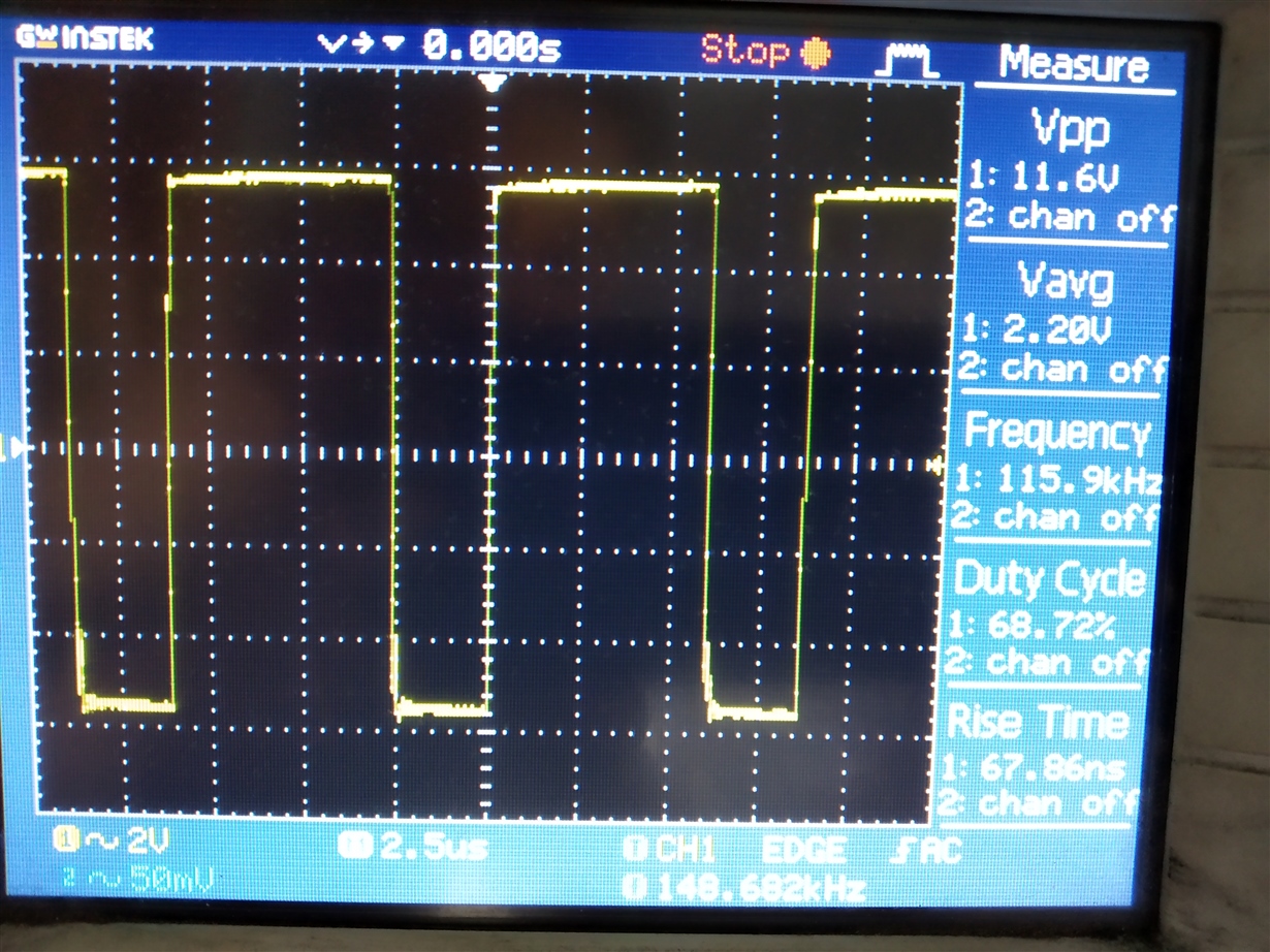
    1st image is I in Waveform

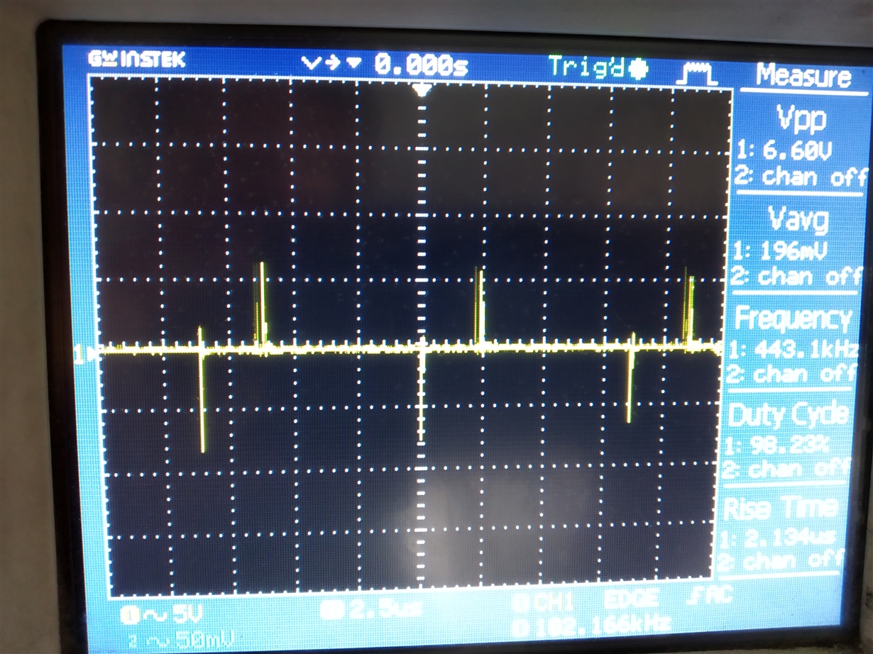
     2nd image is VDD waveform

  • Hi Naveen, 

    Thanks for the waveform. 

    Can you please remove damaged IC and place another UCC27511 driver IC and new FET please capture IN+, Gate and VDD signals during normal operation before failure. I ask this waveform during normal operation because I want to verify whether there is any cause for concerns before failure that might tell us the root cause. 

    But the fact that MOSFET + Driver failed seems to both fail might indicate transients coupling from the high voltage path through the miller capacitance of the FET back to the driver's output stage reason why waveforms during normal operations might help confirm or rule out this theory. 

    How many failures have you encountered? Did you replace IC from initial failure with new driver + FET? Was the failure consistent after 1hr? In other words, have you been able to replicate the failure?

    Thanks in advance for the additional information.

    Regards,

    -Mamadou

  • Hi Mamadou Diallo,

    The VDD and IN+ waveforms which i already sent to you are taken during normal operation with load.

    Yes, I replaced both the driver as well as mosfet and later i have taken the waveforms.

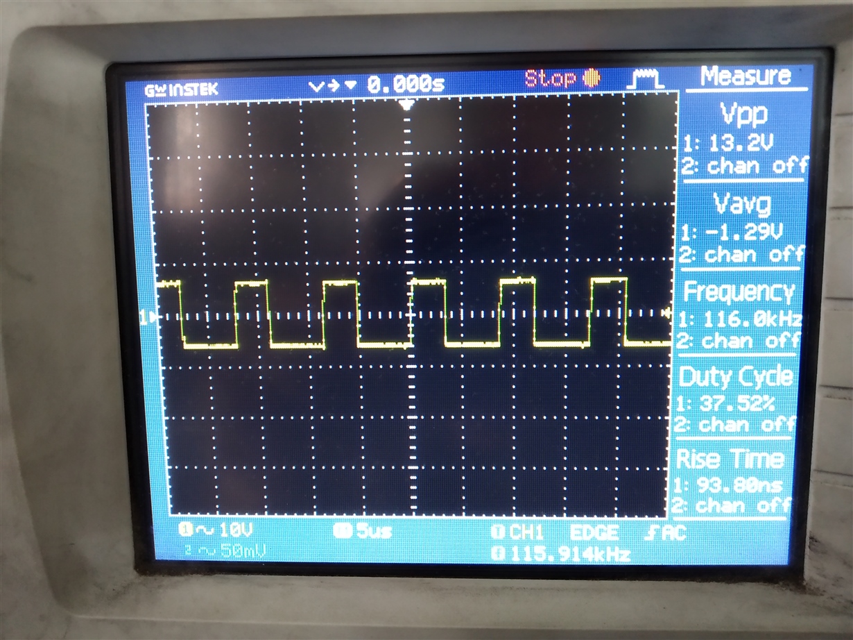
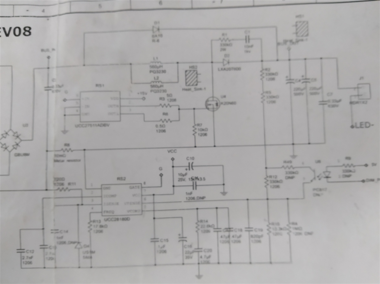
    Here are the mosfet gate waveform and circuit diagram.

    Regards,

    Naveen G

  • Hello Naveen, 

    Thanks for the additional information. 

    Below are my comments from the schematic you shared:

    -I was under the impression that the driver had decoupling capacitors however from this schematic, I do not see the required decoupling capacitors to help filter noise on the driver's supply pin. These capacitors are typically (0.1uF and >=1uF) placed very close to the VDD pin of UCC27511.

    -On the problem description, you seem to mention that failure occurred while switching at 56kHz however looking at the waveforms that you shared, you seem to be switching at 116kHz, 37.5 duty cycle. I asked for the waveform to try and put the driver in similar conditions as during failure conditions to understand whether it is consistent or whether there are signs of potential issues in the design. Please help clarify this item.

    -Driving the 110nC gate charge at VDD=15V and switching at 56kHz will induce gate drive losses of 92.4mW (worst cases no external resistors) which is well within the driver's power dissipation capability so in that case, we can certainly rule out excessive power dissipation from driving the load (MOSFET).

    -From the initial waveforms you shared, VDD seems to be low with intermittent spikes corresponding to the rising/falling edges of the IN signal, I am curious to know why you are not seeing the 15V at VDD if the waveform was captured during normal operation.

    -On the input waveform, you have a 11.6Vpp signal (+/-5.6V at IN+) is there any reason for the negative bias on the input signal? keeping in mind the ROC table shown below: You're providing a -5.6V at IN+ pin while minimum recommended on this pin is -5V. TI only guarantees driver's performance when operating the device within these limits. Please consider adjusting to operate the driver within the specified limits.

    Thanks.

    Regards,

    -Mamadou