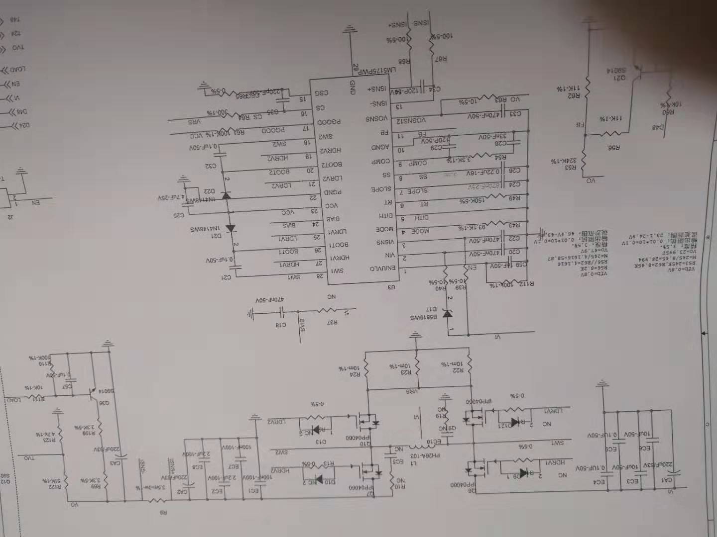
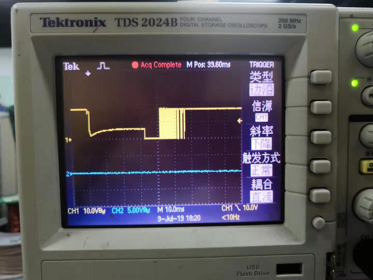
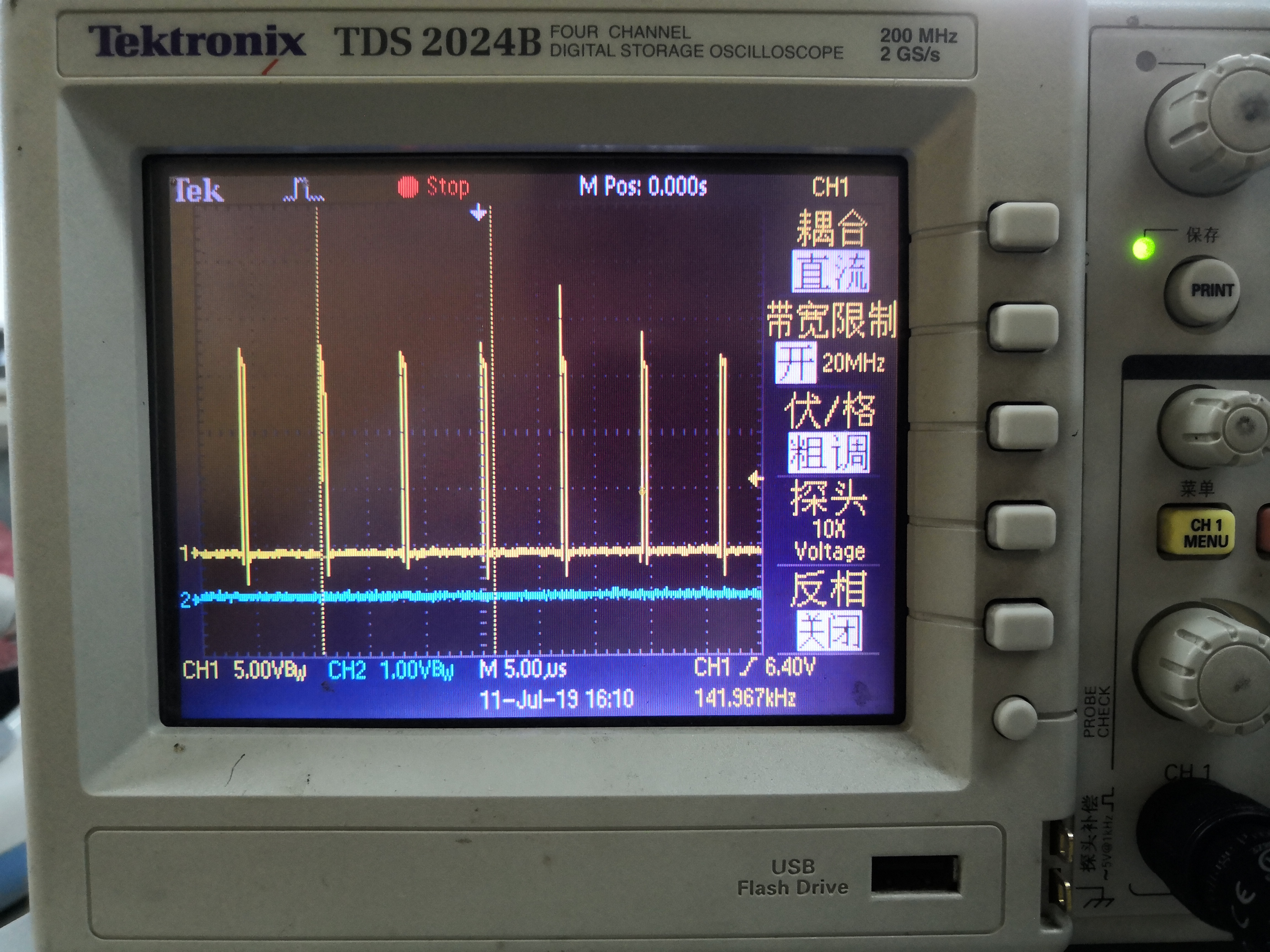
I use the LM5175 in my power degisn. Vin=12V~32V, Vout=24V. If the load in hot swap, the HDRV1 Pin will be damaged. The picture is SW1 (yellow) and SW2 (Blue) after HDRV1 Pin damage. Plaese help to deal with this question. Thanks~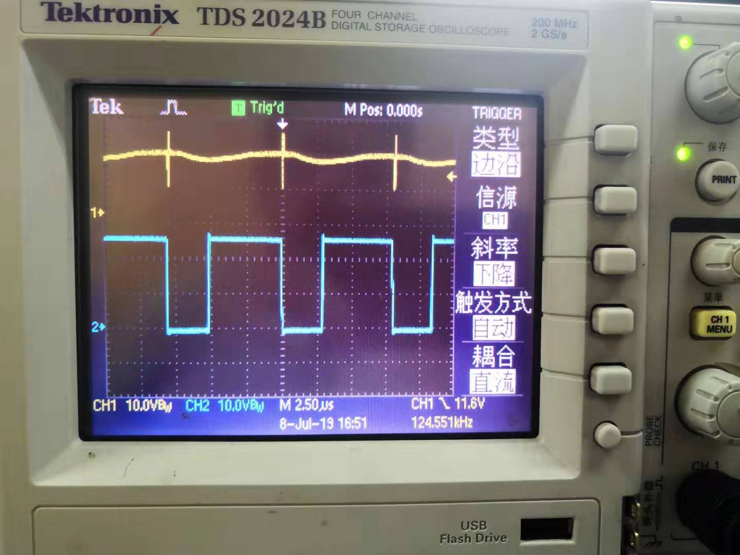
I use the LM5175 in my power degisn. Vin=12V~32V, Vout=24V. If the load in hot swap, the HDRV1 Pin will be damaged. The picture is SW1 (yellow) and SW2 (Blue) after HDRV1 Pin damage. Plaese help to deal with this question. Thanks~