A related question is a question created from another question. When the related question is created, it will be automatically linked to the original question.
If you have a related question, please click the "Ask a related question" button in the top right corner. The newly created question will be automatically linked to this question.
LM5067: Request a Design review and Check a waveform
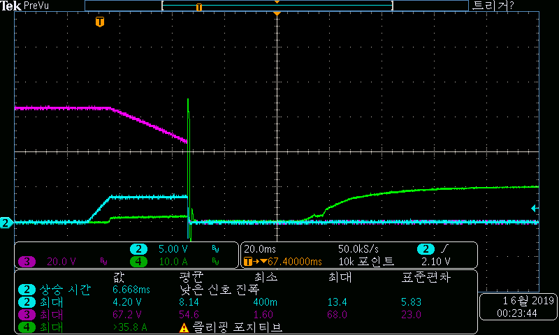
Not necessarily as there can be mismatch between FET to FET. Is there any difference in startup load conditions for the failed board and passed boards?
Are you able to fill the design calculator to check the SOA margin.?
Who is the customer? Did you have local TI field engineer support to have look?
1A) The application report http://www.ti.com/lit/an/slva673a/slva673a.pdf covers the design aspects of hot-swap system. The power limit and dvdt control are covered. Please go through it
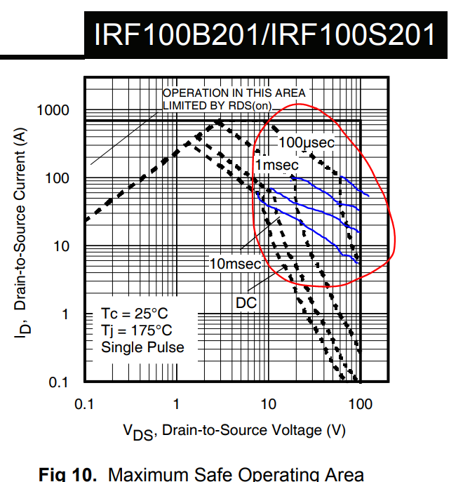
2A) 3A) we suggest to use stronger FET having single slope power limit lines. The FET like IRF100B201 has double slope and are prone to thermal instability during startup, current limit mode of operation. The recommended FET is PSMN4R8-100BSE
FET to FET variation in process/parameter, operating temperature and loading differences may be the reason to see failures on some of the boards. I suggest to take few boards and do all the critical tests at max. Vin (54V), max. operating temperature.
The FET you are recommending can not be applied to products that are currently designed.
The product is a different package and can not be replaced.
The current product package is TO-220.
The second question ,
Currently designed products are not protected in case of short circuit during operation.
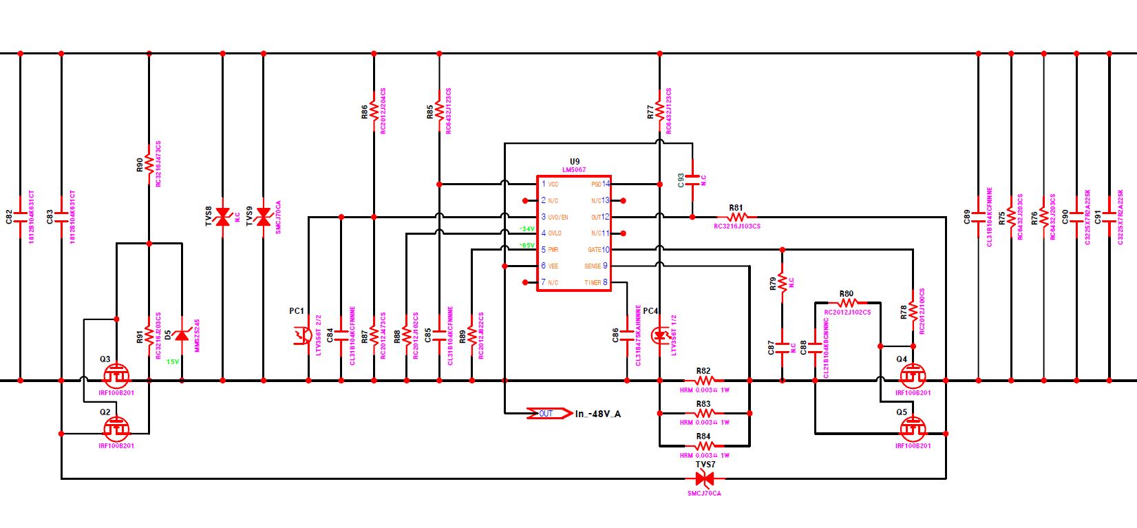
Q4 or Q5 FET is damaged when short circuit occurs.
How can I protect the FET?
Can I review it if I send you the product?
Thank you.
Thanks for the answer. The FET you are recommending can not be applied to products that are currently designed. The product is a different package and can not be replaced. The current product package is TO-220.
The second question I asked was the FET breakdown question in the short circuit. Currently designed products are not protected in case of short circuit during operation. Q4 or Q5 FET is damaged when short circuit occurs. How can I protect the FET? And, Can I review it if I send you the product? Thank you.
You can send me product for verification at our end.
Is short circuit failure repeatable on several boards?
The GATE capacitance will slow down the turn-off process and puts stress on the FET during short-circuit event. Remove any capacitance on the GATE and do short circuit test again.


