


Other Parts Discussed in Thread: UCC20225
Hi,
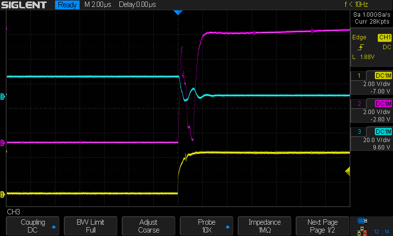
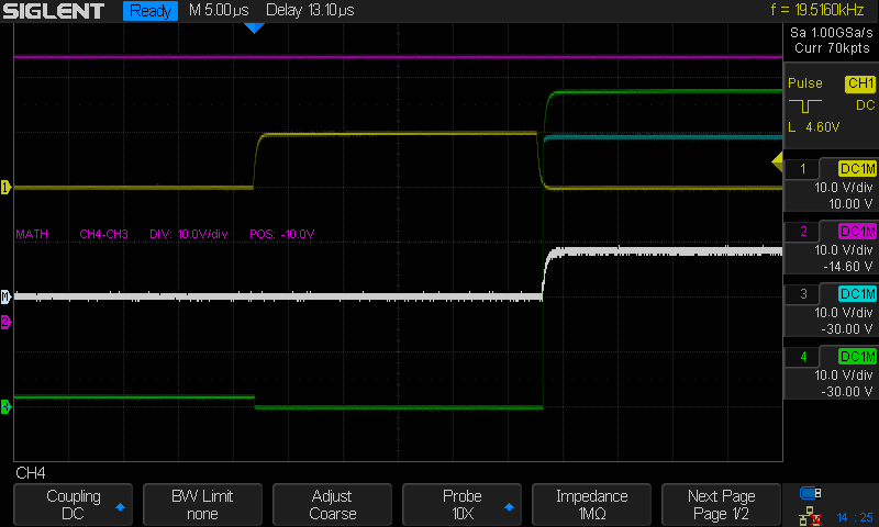
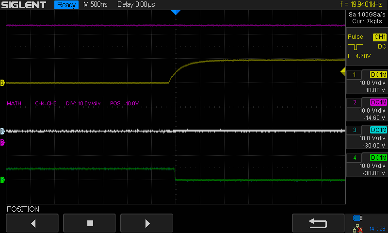
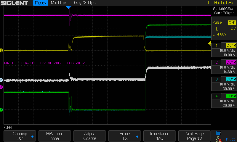
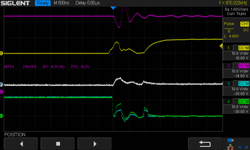
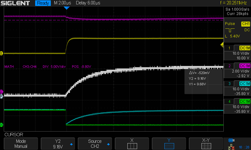
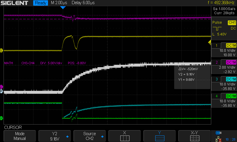
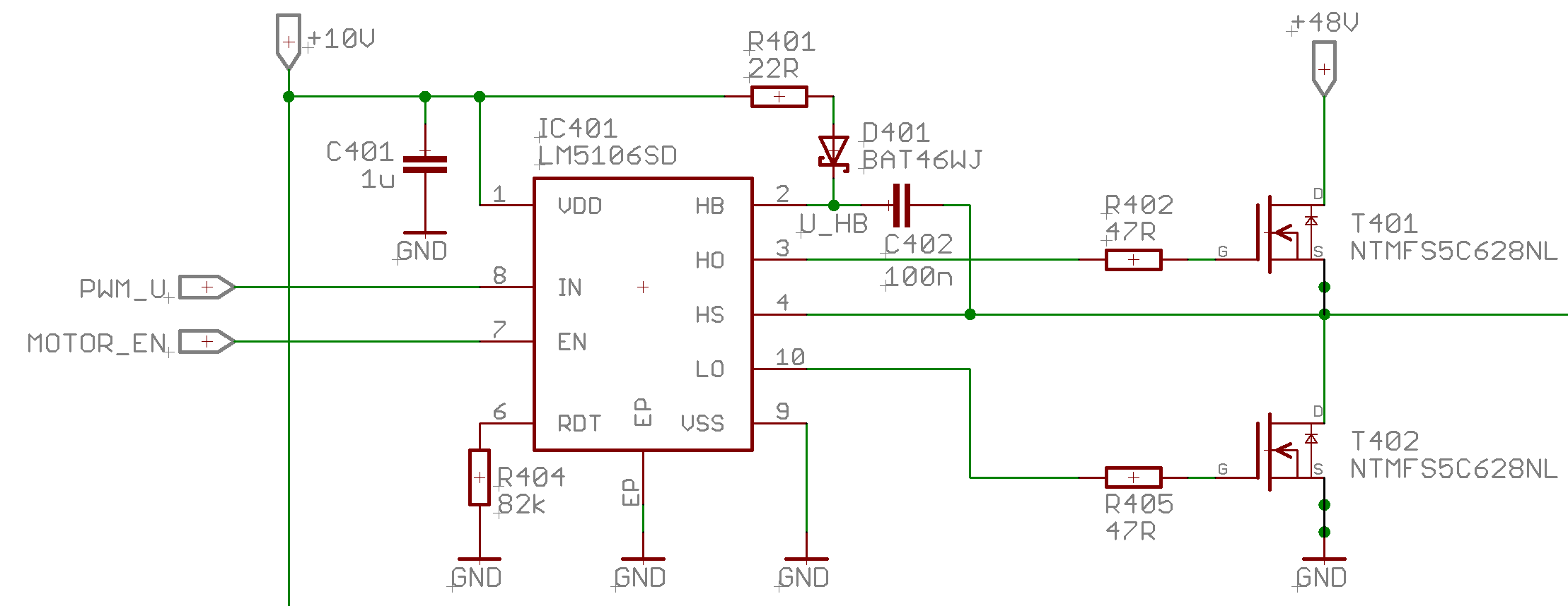
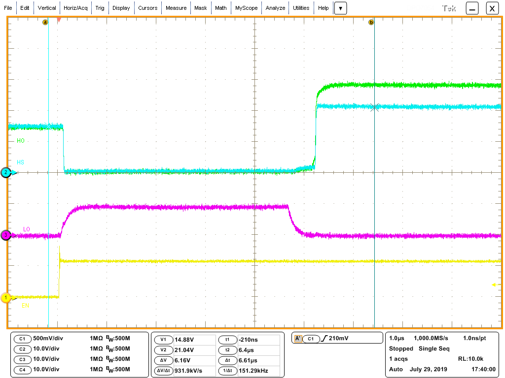
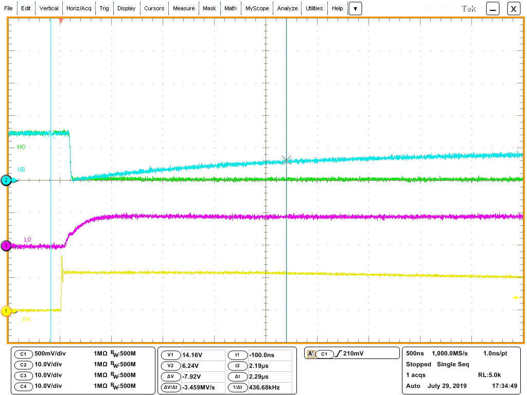
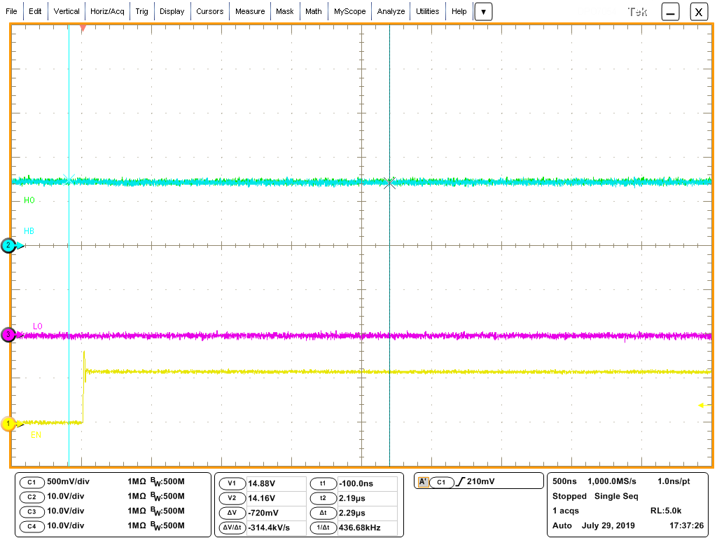
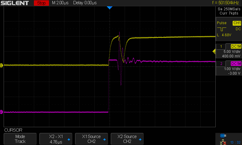
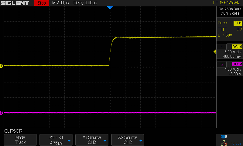
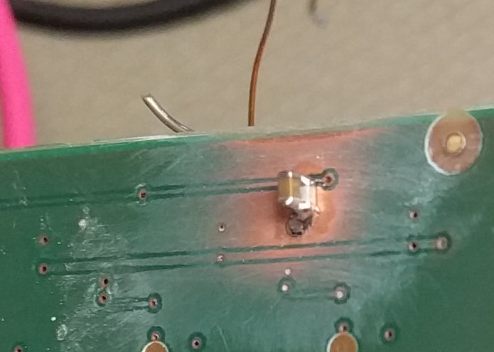
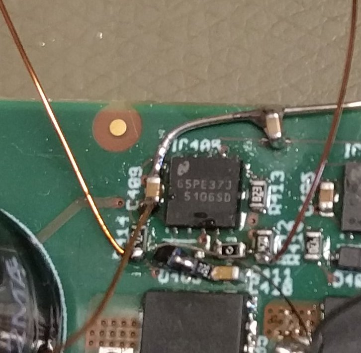
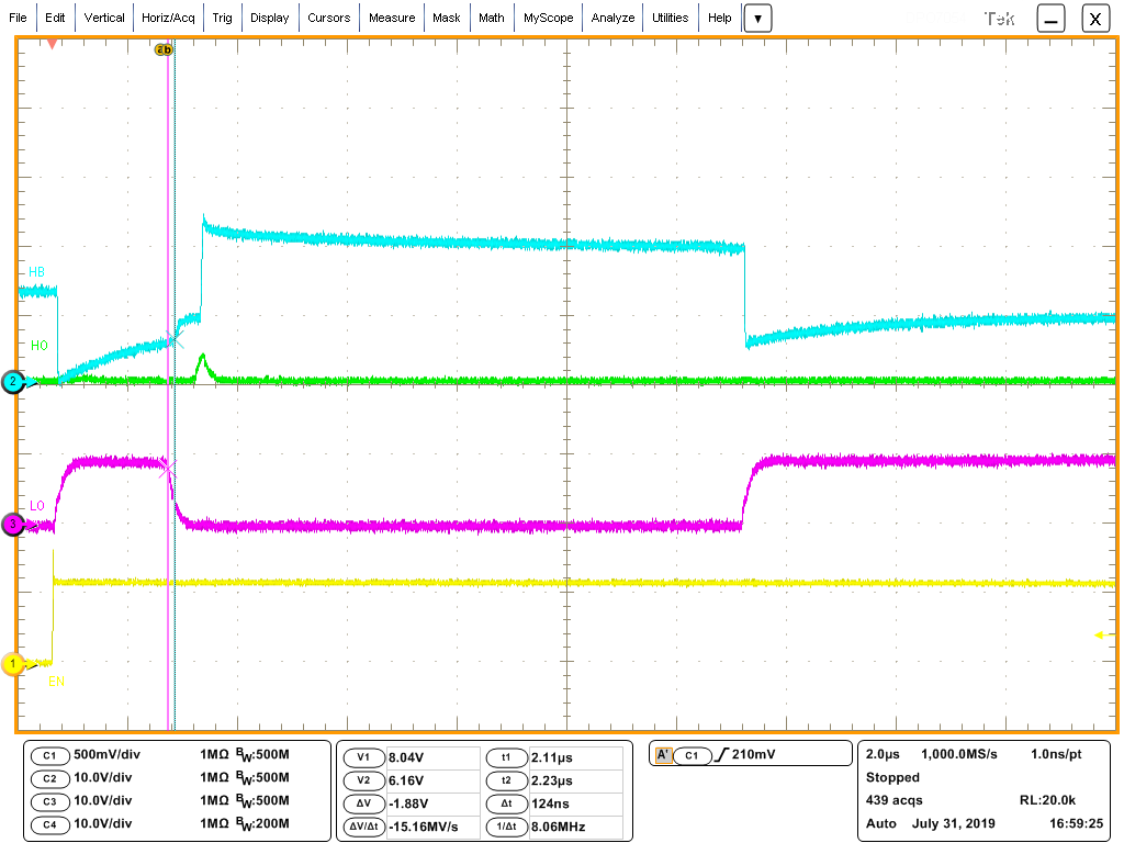
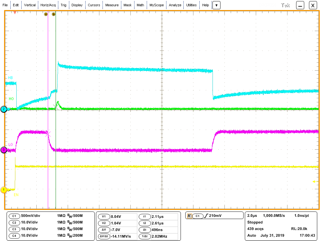
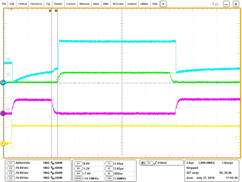
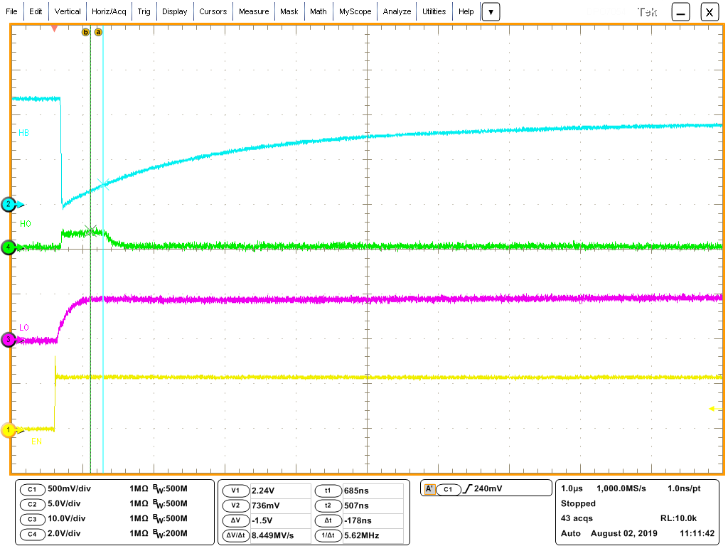
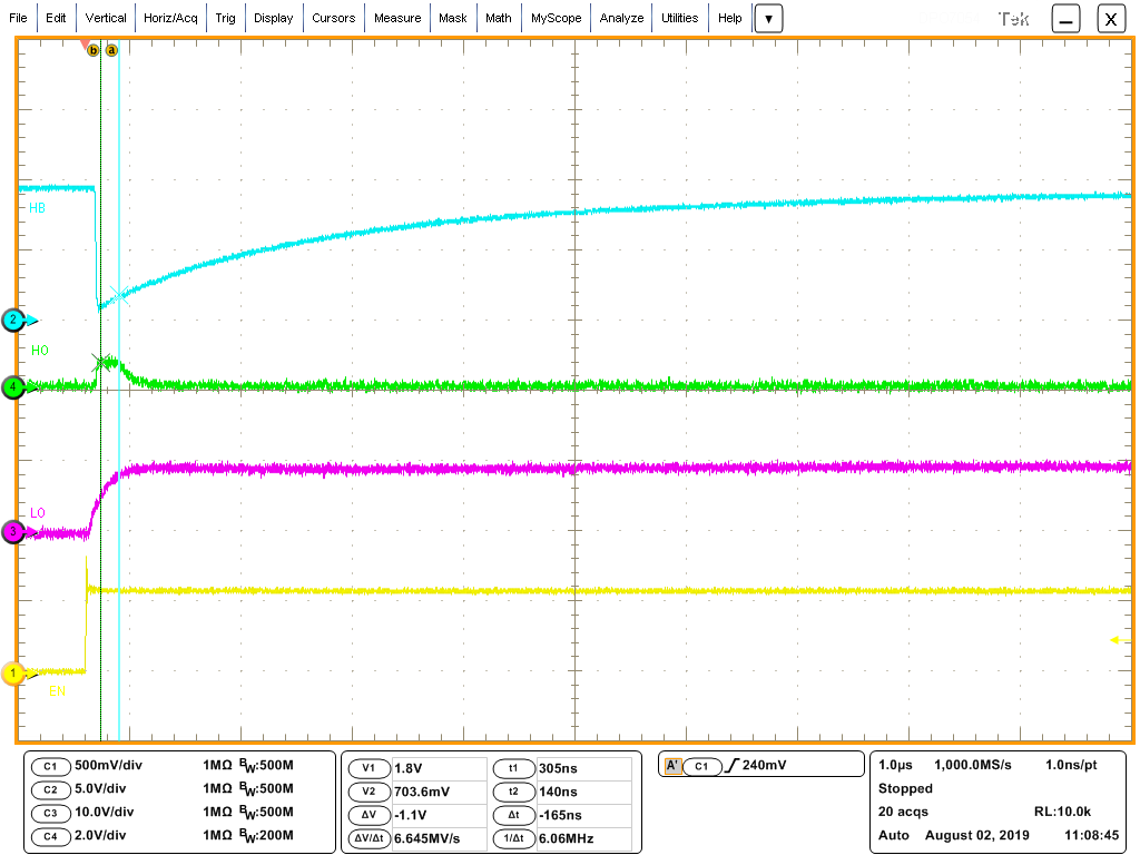
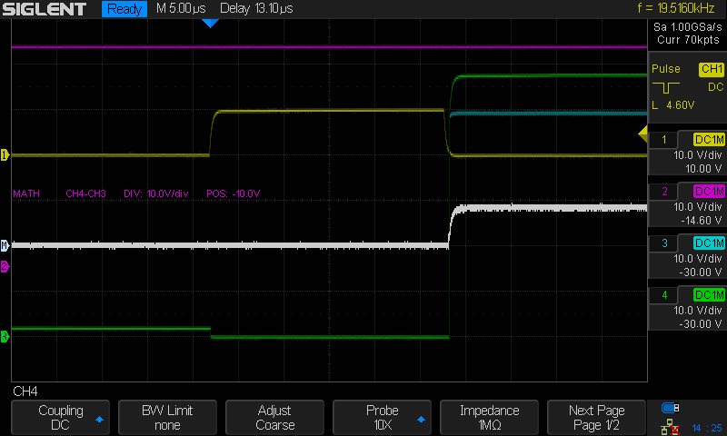
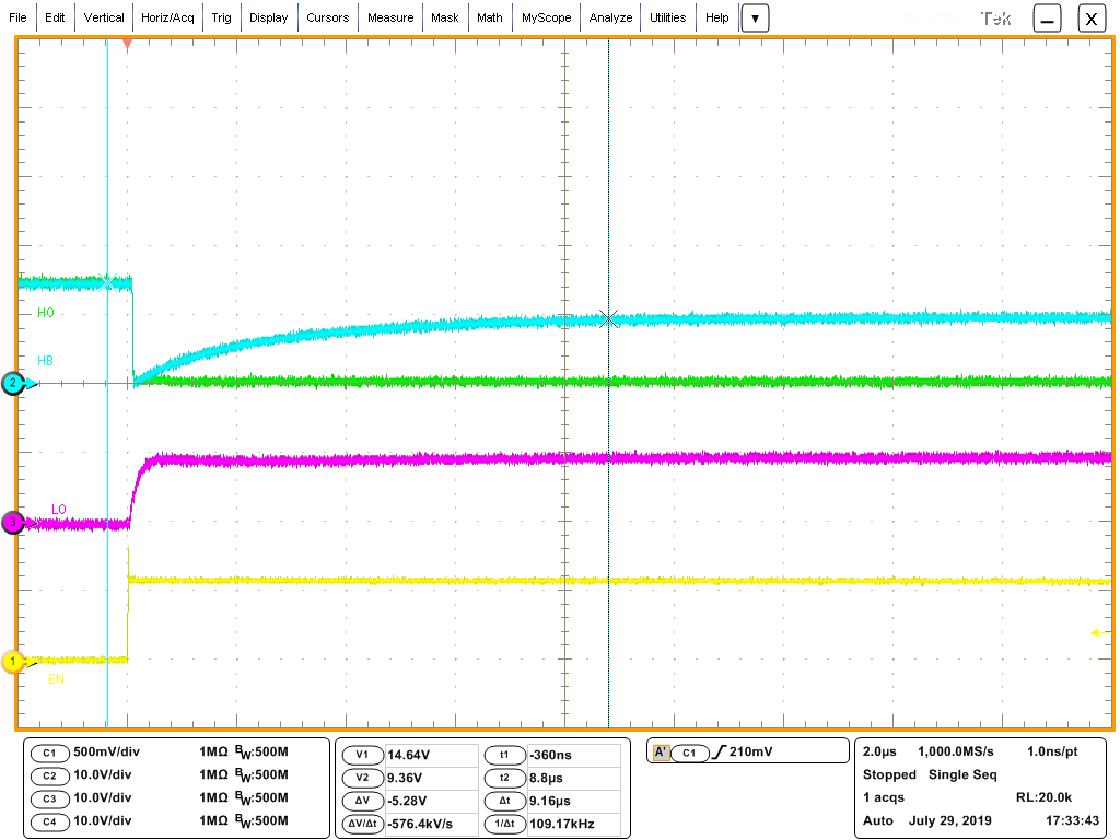
I need to reopen an older case, as we found that the problem that is described there actually still exists.
The old topic is: https://e2e.ti.com/support/power-management/f/196/p/722620/2667359
Original question:

Hi,
I need to reopen an older case, as we found that the problem that is described there actually still exists.
The old topic is: https://e2e.ti.com/support/power-management/f/196/p/722620/2667359


