This thread has been locked.

If you have a related question, please click the "Ask a related question" button in the top right corner. The newly created question will be automatically linked to this question.

TPS92691: After starting up the TPS92691 seems to be stopped by some protection failure

Part Number: TPS92691
Other Parts Discussed in Thread: LM3421

Hello,


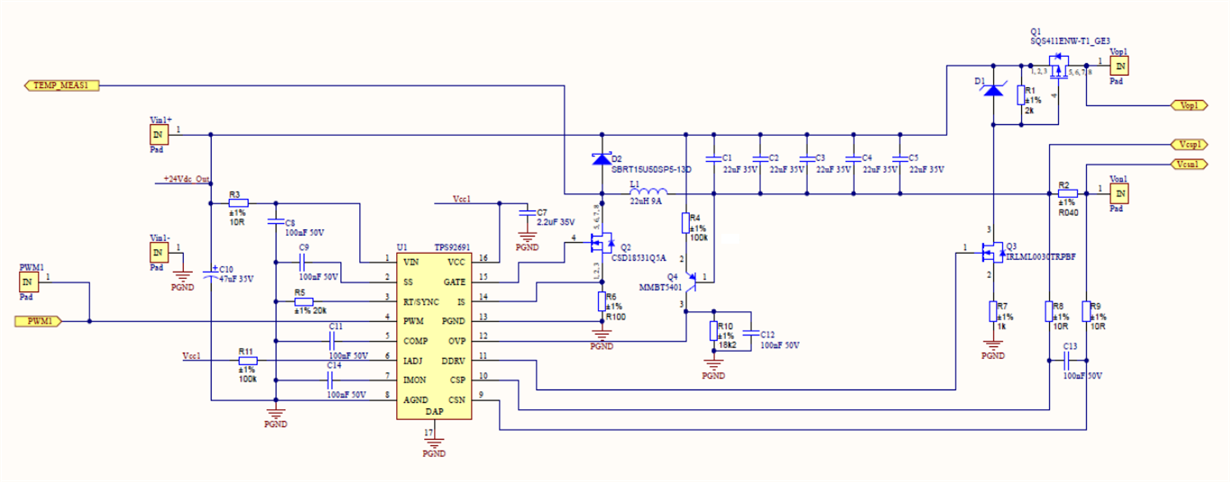
I have designed and performed a low-side buck converter with the aid of TPS92691 part (schematic attached).

Vin = +18V to +26Vdc, Vnom = +24Vdc

Vo = 5Vdc (that is the Vf tipycal led value used as a load)

Io = +4.5Adc.


The fact is that after starting up process the led is not lighting and the converter seems to be off. I just see a few miliamperes in the input power supply.

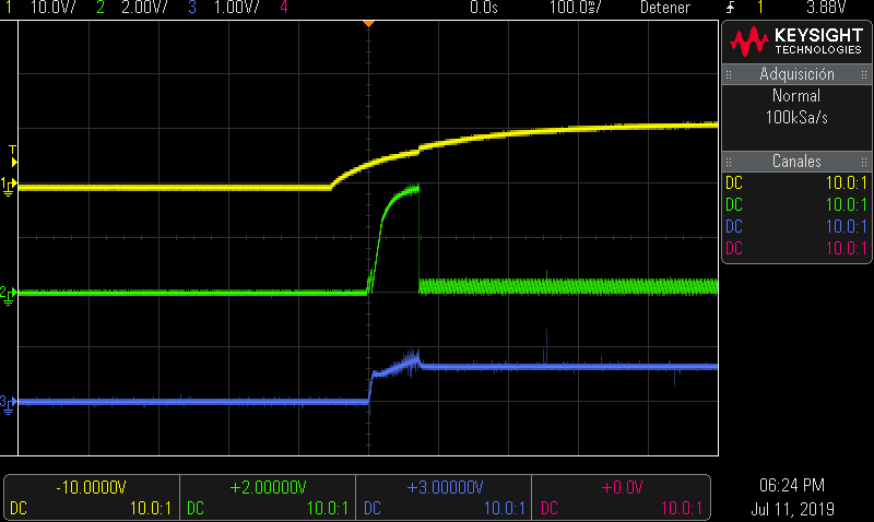
I attach one capture of the oscilloscope, where Ch1 is U1-1 pin (Vcc), Ch2 is U1-2 pin (SS) and Ch3 is U1-12 pin (OVP).

Ch2 (SS) is cut after 75 ms aprox. and it starts to oscillate, the OVP signal is under 1,24V (Vov is almost 8V by design) and it is so far from the limit level.

I cannnot connect 24V to the input because after 10V the converter behaves in such a way and I cannot provide more than 0.7A to the power supply because of this issue.

I am providing either 1KHz pwm dimming signal, 5V or pullin-up with a resistor 100KOhm the PWM pin, which is the case of the capture I attached. The result is the same in both cases.


So, what is happening here? As the led voltage (Vf) is 5V and voltage input is just 10V I can't even see Vsw node operating and the converter seems to not operate really well. In fact i cannot state that the converter is really turned on.

Is there any other protection that is been activated and so this behaviour is justified? I checked the datasheet and saw OVP at starting up process but do not know if there is something else here.

Please, any idea?  Could you help me please?


Regards,

  • Hi Arron,

    The TPS92691 is sensing an over-voltage since OVP > 1.24V.  This is what is turning the TPS92691 off.  Please has scope capture of the output voltage on C1 and compare that to VIN.

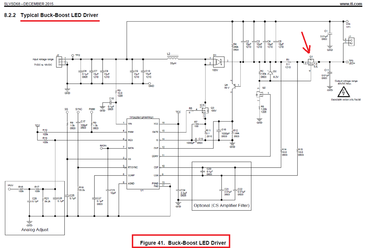
    The PWM'ing FET that you have is not really doing any PWM'ing.  Please follow Figure 41 for this.

    Thanks Tuan

  • Hello Tuan,

    When I wrote my post I asked whether there is any protection failure at starting up process. It was an assumption because I didn't have any evidence of that fact.

    I said that because if you check Vop level captured (1V/div.) you will see that 1.24V level is quite far from been reached (peak max. is 1V at the most! ) . I disagree, I don't think OVP is enabled.

    So, I repeat it again, is there any other protection been triggered? What's wrong here?. Any idea? I am still wondering what is wrong here, i. e. : improper Ccomp value, Css value...etc?

    I don't understand what you suggested to me about figure 41 of the datasheet. It is the buck-boost schematic. Couk you clarify it, please?

    Regards.

  • Hi Aaron,

    Your scope capture on Channel 3...Is that the OVP (pin 12) signal as you have stated...If it is as you described in your message then it will shut down the TPS92691.  The signal (blue) is 3V/div so it's over 1.5V.  The OVP level is 1.24V on pin 12.

    As far as the PWM'ing FET (Q1) is concerned on your schematic...You have the connection wrong with it connected to the Vin while out Figure 41 has it different.  Q1 FET intrinsic diode is always on with anode always biasing On and you cannot turn the FET off.  Please change your design to the recommended Figure 41.

    Thanks Tuan

  • Hello Tuan,

    Let me clarify you something about the capture scope because I think you're a bit confused. Look at the top of the picture, you'll see Ch1 10V/, Ch2 2V/, Ch3 1V/ and Ch4. This is the setup of each channel and I DO NOT HAVE 3V/div in Ch3. You are looking at the bottom of the picture and this is not the V/div setup.

    I have also take a measurement in OVP pin and it is under 1.24V level. Let me clarify you that Vin = 10V aproximately, it is not 24V yet.

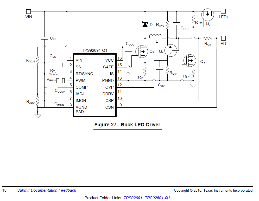
    As for your suggestion about Figure 41. This is the Typical Buck-Boost Led Driver schematic and I am not using a such configuration, I am setting a Buck Led driver and the scheme is not the same. If you see Figure 27, the schematic recommended in the datasheet is exactly the same that I am setting in my design. I attach you both schematics and if there is an erratum in Figure 27 schematic, please let me know it.

    Anyway I have discovered the root of the problem and some other things that really disturbs to me.

    First off, regarding OVP calculations, as you can check in my design R4 = 100KOhm an R10 = 18k3.

    This comes from (pages 29 and 30, datasheet):

    Rov2 = (R4) = Vov(hys)/20/10e-6

    Rov1 = (R10) = ( 1.24 / ( Vo(ov)-1.24 )  * Rov2

    I selected Vov (hys) = 2V and Vo(ov) = 8V

    The fact is that when I tried to startup the driver (Vin = 24V), the signal that I measured was about 3.7V in OVP pin!. After that, I set Rov1 (R10) to 12k4 and still got 2.64V!!.

    It is quite simple, it is just to apply Ohm's law...Ok, but how can this be if the Rov2 and Rov1 formulas are setting this according to 1.24V, hysteresis and Vo(ov)? Are these formulas Ok?.

    I finally set R4 = 100kOhm and R10 = 3k3Ohm following Ohm's law and the OVP pin is lower than 1.24V limit threshold.

    OK PROBLEM FIXED, now I can startup the driver and apply a PWM dimming level...

    BUT, again after applying a certain pwm % level (20% for Vin = 24V) the driver shuts down again. The problem is that Vis peak level is higher than 525 mV.

    So let me show my calculations again according to the page 29 (datasheet):

    Ris = (2 x VsL x L x fsw) / Vo (max) = 0.84 Ohm

    Ris = (Vis(limit) - VsL x Dmax) / IL(pk) = 0.097 Ohm

    Vsl = 0.2V, L = 27uH (in my desing is 22uH), fsw = 390KHz, Vout (max)= 5V

    Vis(limit) = 525mV, Dmax = 0.32, IL(pk) = 4.725A

    The datasheet recommends to take the lower Ris valuem, so I took 100mOhm as you can check in R6 resistor.

    So, again, how can this be? Am I wrong or not? What I also checked is that the driver is out of regulation because 10% dimming level is not the 10% output current value, is higher and little changes (1%) of dimming increases a lot the output current.

    In summary, can you clarify what I have described here, please? Could you help me? I need technical support, this is a new design and I am interested in it.

    Regards

  • Hello Tuan,

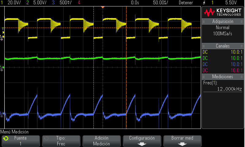
    I also attach you a scope capture for a 12% dimming level at 12KHz frequency and 5V level voltage.

    As you can check on Ch3 (500mV/div), this is Vis peak value which is almost 525mV and the driver is near to be shut-down.

    Ch1 (20V/div) = Vsw node and Ch2 (5V/div)= SS pin.

    This is the evidence I have talked you about before.

    Regards

  • Hi Aaron,

    My apology for the mis-understanding.  On figure 27 of the data sheet, the CSP and CSN is reversed and I assume that's how you also have the CSP and CSN reversed on your schematic.  We will correct this on the next revision of the data sheet.

    So let's swap the CSP and CSN connections first and see if that helps you.  Please have the COMP (pin5) voltage on your scope capture above along with the current probe on the LED.  If the switch node is running at the PWM cycle frequency (12 KHz) then the loop can be saturated and you are not getting the the current control level.

    The equation for the OVP should be good...The reverse connection on CSP and CSN can cause high current level and cause the shut down to happen.  First just use your lower value of 3.3K for R10 just to basically put OVP at really high voltage so it's not complicating your debugging.  Then go back to your original calculated value after all the debugging is done.

    The PWM frequency at 12KHz is quite high and this can be an issue with the level shift gate drive for the PWM'ing FET (Q1) with narrow duty cycle.  What is the application that you would need to run at that high of a PWM'ing frequency?

    Please let me know things work out.

    Thanks Tuan

  • Hello Tuan,

    The driver is intended to applications that requires a led of 5V (Vf) in low-side configuration and a frequency dimming 10KHz to 20KHz.

    I performed the swap in CSN and CSP signals in my circuit cutting nets and using some wires.

    The result was unsuccesful because I still have the same problems, despite being welll configurated now.

    I mean, there is no output current regulation, the output current changes with the frequency dimming and the converter is unable to start-up at 24V because the level at Vis pin reaches a peak higher than 525mV. This value is specified in the datasheet.

    I changed 3.3KOhm and increased to 5k6 but and nothing wrong happened, good news. Then I performed the following changes but they were all unsuccesful:

    For fixed/pulling up pwm signal to +Vcc

    • I changed Ccomp (C11) component and used values from 10nF to 100nF as the datasheet suggests.

    Test Result: Ko, there were no changes.

    • I changed Ris (R6) from 100mOhm to 15mOhm with the purpose of allowing the startup process and avoid the 525mV.

    Test Result: Ko, when starts up, Vis reaches the value of 525mV.

    • I changed Rcs (R2) to check whether the driver is able to set another output current properly. Changed R2 to 180mOhms to set a Io ~ 1A.

    Test Result: Ko, it seems to me that there is no current sense differential amplifier operating at CSP and CSN pins!

    • I also changed pull-up resistor Vadj from 100kOhm to a resistors network to set a certain current as datasheet describes.

    Test Result: Ko, nothing changes because the output current does not follow this setup and reaches higher values.

    • I changed RLS2, RLS1 and Zener diode (R1, R7 and D1, respectively). RLS2 = 47KOhm, RLS1 = 1KOhm and zener diode changes from 3V9 to 10V. 

    Test Result: I could notice here how the rise and fall times changed and consequently the heating at the Q1 PFET decreased too much.

    So, I think that this satisfies the operating function of the mosfet. Correct me if I am wrong, please.

    In summary, I still see a converter that seems to be in open loop because it is never regulated and does not responds to any change. Is there any other erratum in the schematic or in the datasheet? Are the formulas Ok? I ask you for this again because it seems that the Ris value, Rcs value and the current sense amplifier are not aligned to setup an adequate control loop regulation. PLEASE, EXPLAIN IT TO ME, BECAUSE IT SEEMS THAT CURRENT SENSE AMPLIFIER NEVER OPERATES.

    As you can check in the attached scope captures, the switching node is running at the PWM cycle frequency (20KHz in this case) when dimming. But why? I cannot understand it, I assume that it is saturated as you said before, but which event or thing is producing that? I have also checked that when I am dimming, in the main mosfet Q2 gate there is a signal of PWM cycle frequency, not the fsw of 390KHz. In fixed mode, I see 390KHz. PLEASE EXPLAIN IT TO ME.

    Of course I changed the driver U1 several times and I saw the same behaviour. Nothing changed.

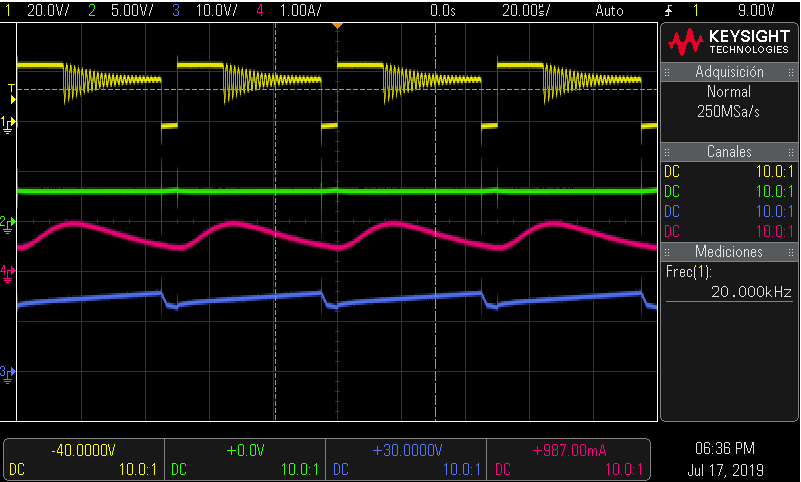
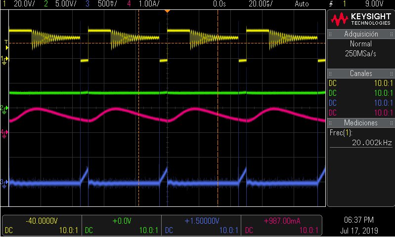
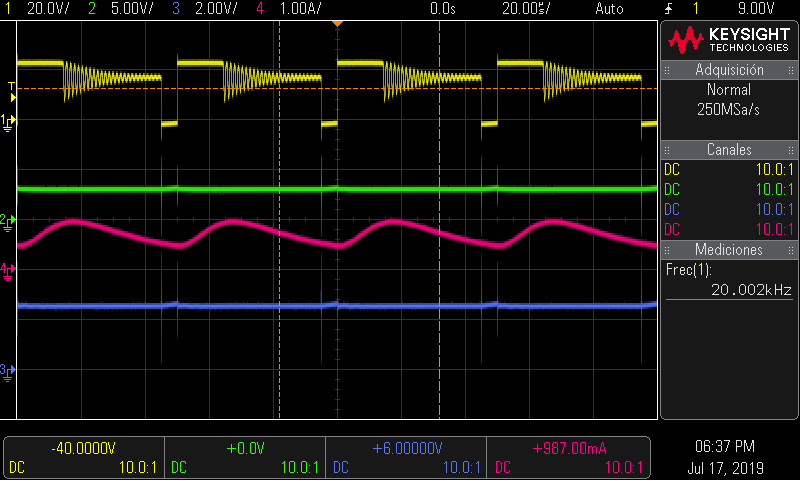
    I attach all the scope captures I took for your checking (20KHz, 5V level, 10%, Vin = 24 V, In = 0,190A, Io = 660mA)

    When dimming I cannnot reach more than 30% without reaching 525mV peak limit and at this dimming level Io is almost 4A.

    Please, need your technical support because this is driving me insane all this makes no sense.

    Regards,

    Ch1 = Vsw
    Ch2 = SS
    Ch3 = Io
    Ch4 = Vanode diode zener

    Ch1 = Vsw
    Ch2 = SS
    Ch3 = Io
    Ch4 = Vis

    Ch1 = Vsw
    Ch2 = SS
    Ch3 = Io
    Ch4 = Vcomp

  • Hello Tuan,

    I have received no comment to my last post.

    Have you read it? I assume you're checking all I have made and you're reviewing it all.

    Please, really need technical support with this issue.

    Regards,

  • Hi Aaron,

    Is the PWM's input running during Soft-Start?  If it's running during Soft-Start then it could explain what is happening.  The other question is whether you are using the PWM pin to disable the part then re-starting and enabling the part.

    Please look at PWM input when power is first-applied and PWM input.  If you can try and have PWM not running during soft-start to see if it helps with your issue.

    Thanks Tuan

  • Hello Tuan,

    I have told you that I tested it im two ways, pulling - up tge pwm input as datasheet suggests and with a pwm input.

    Pulling - up the pwm input to Vcc signal produces an excess os Vis peak voltage (525mV) for Vinput =24V. That is why I asked you before whether the formula for getting Ris was Ok. I had to redice it to  properly startup and finally it does not work either.

    With pwm input I start-up the part and then I drive the pwm input. The part starts up and them after a dimming % duty produces the waveforms I've attached you before. It does the same if I try to startup the part with the pwm input enabled.

    I have tried it all and the result was unsuccessful.

    Please, another idea?

    Regards,

  • Hi Arron,

    There are a few things that can be going on here:

    1.  For the case of PWM being pulled up high (100% ON): If you tried lowing RIS and it still failed with the larger CComp cap then the issue can be the inductor saturation current.  Please please a current probe on the inductor with one side pull up thru a wire for the current probe.

    2.  For the PWM'ing case: The PWM'ing frequency is quite high at 12KHz or 20KHz.  At this PWM frequency and narrow pulse you will not be able to ramp up to the controlled current level.  We do not recommend PWM'ing at this high frequency and narrow duty cycle.  I've mentioned about the high PWM frequency previously.

    Thanks tuan


  • Hello Tuan,

    As you know in a step-dowm converter the IL current is the output current, so it is not strictly necessary to pull-up with a wire the inductor.

    Despite that, I followed your tip and did it and I saw the same output current Io waveform for the pwm dimming frequencies mentioned (10KHz to 20KHz). The current waveform is attached before in this thread.

    But, there is something about output current Io or inductor current IL that it is indeed not correct. The current waveform is still showing a saturation shape. Why?  I'll try to explain it all I've seen.

    One thing I forgot to mention here is that I tested 500Hz and 1KHz dimming frequencies and the result was a severe blinking in the led string and a strong noisy sound (it seemed logical for the noise because of the audible band frequency used). If i tried to increase dimming always got an unregulated output current value and a more severe noise. But I never reached 99% value...

    When I reached 99% value the current waveform Io and the converter behaviour changed it completely. It seemed as if the current sense amplifier hitched the loop, so to speak, and then If I tried to reduce the duty the current waveform was Ok. In fact, If I tried then to increase the value again the driver was able to did it.

    I attach you all the waveform evidences to understand it. The inductor value and component selected is a powder iron core and has a saturation current up high the rms current value in the circuit. Anyway I changed it for a ferrite core of similar values and got the current waveforms attached.

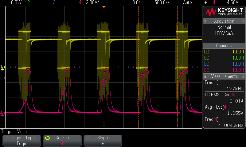
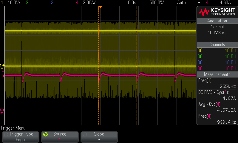
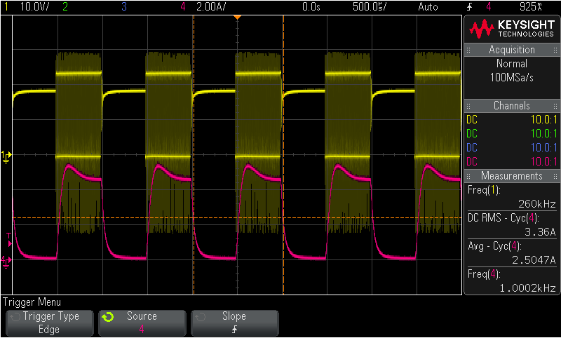
    Ch1 =  Vsw, Ch4 = Io. Waveform at startup for a dimming frequency of 1KHz.

    Ch1 =  Vsw, Ch4 = Io. Waveform at duty 99% for a dimming frequency of 1KHz and seemed to be Ok after current sense hitched-loop.

    Ch1 =  Vsw, Ch4 = Io. Waveform at duty 50% for a dimming frequency of 1KHz and seemed to be Ok.

    For improving startup I've added a resistor in parallel with Ccomp to smooth the raise part of the waveform but I still have to adjust it.

    Am I wrog with this? Any tip here?

    I still have problems to startup the driver when pullin-up to +Vcc pwm input signal. I still have to reduce Ris. What's wrong here?

    Another issue is that, changing the dimming frequency means changes at ouptut current rms value, how can this be? Is that normal in this driver? It is due to a problem in the compensator network?

    Finally, the linearity of the part is not quite accurate, it seems to be ok for 50% and 100% but nof for 10%, 30% and so the like. Maybe is due to the compensator network adjusting, isn't it?

    Could you help me, please?

    P.D.: I know you mentioned before the use of high frequency dimming (12-20KHz). The fact is we need a frequency dimming a bit high to avoid noise of low frequencies used and for a requirement. I've asked you in another thread if the part (TPS92691) was able to be used with such a frequency dimming values and you told me that the part was able to. But there is no problem. We could dimm with adj pin if needed as an alternative but first we have to fix the problems I'm reporting to you.

    Regards,

  • Hi Arron,

    1.  I did not mentioned that PWM'ing at 20KHz is OK on the other post:  Please see my answer again:

    The 12KHz you are PWM'ing along with narrow duty cycle can be an issue here since it's really fast PWM'ing.  I've asked a question in your other post about you  application here and whether you can go lower on PWM frequency.  For LED and headlight application, the PWM frequency is usually from 120 Hz to 400 Hz.

    From you results...this is your real issue.  Beyond this you will have to trouble shoot your own design.

    Thanks Tuan

  • Hello Tuan

    After reading your last comment I am a bit stunned. Let me tell you.

    I am not here to be angry and to show fury for any commented post, I think you have taken it personally and have focused only on P.D. comment I wrote about PWM dimming frequency. I think the goal of the forum is not this and reading your comment it seems to me you have answered in a bad way. Let me tell you.

    Tuan,

    I said : "I've asked you in another thread if the part (TPS92691) was able to be used with such a frequency dimming values and you told me that the part was able to". You can check it in another thread not in your last post as you said it to me. The thread was "TPS92691: PWM dimming frequency range". You commented there exactly this:

    "Hi Aaron,

    The PWM circuit will accept the 20KHz pwm frequency but the main limitation is the gate drive of our driver and whether it can drive the FET that you have externally.  The simple way of thinking is what you mentioned above with the 5RC time constant but fir a FET it’s related more to gate charge to be exact.

    Thanks Tuan"


    Ok, I tested it using the same FET I have used for a 20KHz dimming in a step-down converter with LM3421 driver. There was Ok and operated well there.

    Unfortunatelly here didn't worked and I realized about the problem (maybe due to gate driver as you said) and told you about using adj pin for dimming purposes. I think it is all quite clear and you didn't have the need of answering in such a way.

    Tuan,

    I recall you that the datasheet still needs to be updated and there is an important erratum related to CSP and CSN pins that forces me to perform a new pcb. Not all is due to a powder iron inductor and some other adjustments. This is not only my real issue as you said. I think the entire post is quite profitable and should be useful for the rest of users. That is the real goal of this forum, to me.

    On the other hand, there are some questions that I assume and don't expect you are going to answer like the output rms current variation due to the change of frequency dimming. For example I tested it and notice that from 100 to 500Hz the output current changes. The poor linearity I checked, Ris needs to be lower than the one suggested by the formula and some others you didn't tell me anything because you focused just in PWM dimming comments...

    No problem, it doesn't matter (but in fact it really matters).

    Of course I deal with my own design and I care of it. I do not hope anybody else do it for me. I almost have the driver operating fine, when I finnished I will attach you all the waveforms.

    P.D.: Aaron please not Arron... You typed it wrong too many times.

    Regards

  • Hi Aaron,

    I am really sorry if the answer came across that way to you...It's definitely not meant that way at all.  As I mentioned, the real issue here is the 20KHz PWM'ing.  Our part, the TPS92691 will accept the 20KHz and drive the DDRV pin accordingly but the issue is the power stage along with external level shifted gate driver for the PWM FET will not be able to response to it along with narrow duty cycle.  This is simply the message I am trying to get across. 

    There is a matter of sampling theory also here that we did not go into.  If you are PWM'ing 20KHz with 10% duty cycle for 5uS ON time.  During this 5uS, the feedback current (CSN and CSP) has to reach the controlled current level for at least 4-5 pulse of your 390KHz power stage switching to keep the loop happy and in control.  So for 5uS this is not possible with what you have so the loop goes into the 100% duty cycle during your PWM ON time and that's what you are seeing.

    There were a lot of data along with questions that you have and it's really the narrow PWM'ing pulse that is causing you all this issue.  So my comment as to all your other questions was for you to trouble-shoot your design as to why.  That's all.  We really did not meant for it to be that way and I am here to help you with the design as best as I can.

    I'll also reach out to you on your email account on this issue.

    Thanks Tuan

  • Hi Aaron,

    I've received your email and will resolve this issue via Email so we will close this post.

    Thanks Tuan