This thread has been locked.

If you have a related question, please click the "Ask a related question" button in the top right corner. The newly created question will be automatically linked to this question.

UCC28950: ZVS operation during turn-off

Part Number: UCC28950
Other Parts Discussed in Thread: LM5045, UCC25600, UCC28951,

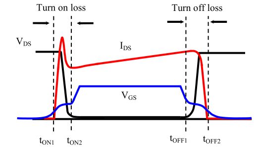
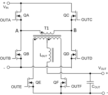
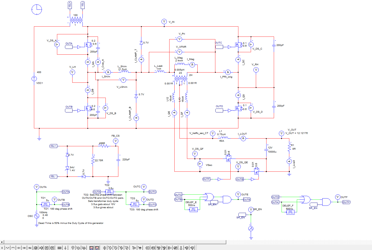
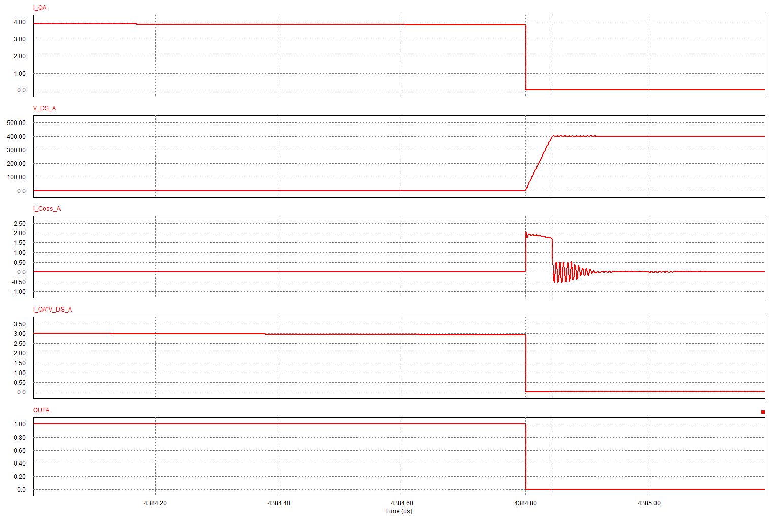
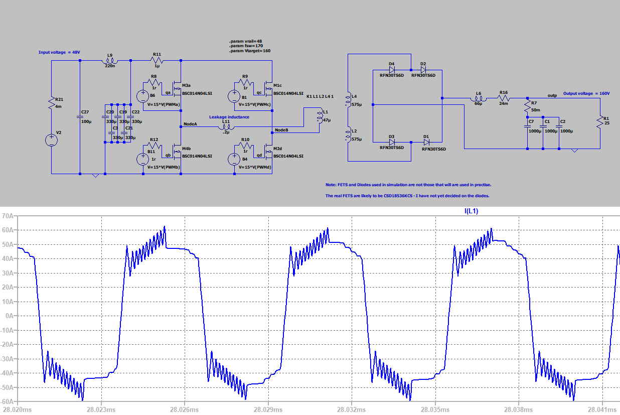
This is my first phase shift full bridge project and I am having some trouble understanding how low-loss switching is ensured when bridge FETs turn off. Especially in the passive leg, when the circulating current is at it's peak. I can find no explicit mention in the literature (maybe I'm missing it) - although much seems to be made about turn-on. Is it simply the capacitance at the leg middle node holding the voltage while the current through the FET drops? In which case the capacitance needs to be large enough to soak up the circulating current without the voltage rising significantly for the Tf duration of the FET.

My problems are probably made worse by the fact that my converter is 500W+ running from a 24V source, so the currents are absolutely huge - so if any has any suggestions for a more appropriate topology (must be isolating), then that would be appreciated.

  • Hello Kevin

    The first thing I'd say is that most PSFB applications run off 400V and are between 1kW and 5kW. You are running it off a 24V input rail so the switching losses you are avoiding are much less significant than they would be at 400V (24V^2 << 400V^2).

    This means that you do have alternatives - a half bridge LLC (UCC25600 or UCC25630x) or a hard switched Full Bridge (LM5045) are possibilities.

    Having said that, the PSFB will work at this power level and I assume that you chose it for a reason.

    Here's some information about the energy available to drive the switch transitions /cfs-file/__key/communityserver-discussions-components-files/196/7725.ZVS_5F00_SubSet.docx

    Just prior to any of the transitions one of the switches turns off. The current which was in that switch continues to flow, driven by stored inductive energy. This current then charges the switched node to either Vin or Gnd (depending on the which switch was turned off). The node is then clamped by the body diode of the other switch in the leg. This switch is then turned on.

    /cfs-file/__key/communityserver-discussions-components-files/196/0511.PSFB-Switch-Transitions.pptx

    There are a number of different terminologies used depending on which publication you look at. Here’s a list of the ones most commonly seen.

    QA, QB: Called PA or Passive/Active or Leading or Left Leg.

    QC, QD: Called AP or Active/Passive or Lagging or Right Leg.

    • The term Passive/Active leg is used because this is the leg that transitions to initiate a new switching cycle. The transformer changes from being a passive state where it is not transferring energy to the secondary to an active state where energy is being transferred.
    • The term Active/Passive leg is used because this leg switches to end the energy transfer active state and enter the passive state.
    • The term PA means Passive/Active
    • The term AP means Active/Passive
    • The Leading Leg is the leg that switches at the start of a power transfer cycle at the Passive to Active transition.
    • The Lagging Leg is the leg that switches at the end of a power transfer interval at the Active to Passive Transition.
    • Left and Right Legs. The names are obvious BUT the function of the left and right legs depends on how the schematic is drawn and which signals are used to drive the switches so these terms can be misunderstood.

    Please feel free to update this post if you have any further questions

    Regards

    Colin

  • Hi Colin

    The switching losses are proportional to the product of voltage and current, so in a hard switching converter, at turn-off, there is a finite time for the current to fall and as it falls, the voltage across the FET rises. For the period that this fall and rise overlap, the device is dissipating power. This is true of all the FETs in the H bridge. The picture below comes from a Fairchild appnote about hard switching, but it's a nice picture to illustrate my point.

    I understand how the turn-on losses are obviated by the resonant 'kick' setting the voltage across a FET to zero before it's turn-on, but as far as I can see the turn off losses are not addressed - I can see no difference between a hard switching converter and a ZVS PSFB converter for the turn off process for each of the FETS. So my question remains - is this a correct analysis or have I misunderstood something?

    If it is a correct analysis can anything be done about it?

    I can see that my comment about the passive leg might have been misleading - wrong terminology - I meant the CD leg, which has to switch more current than the AB leg.

    I have an extremely ambitious target for the size of this converter, so I am extremely sensitive to any losses whilst at the same time having to switch currents in the region of 100A. I have looked at the LLC topology and the possibility of rigging the LLC values to achieve zero current switching in a crude simulation, that looked promising, but I imagine it would get extremely complicated trying to maintain this over load and input voltage ranges and also try to persuade a controller to work like this. I'm not quite ready to give up on PSFB yet.

  • Hi Kevin

    First of all, IF you can operate a LLC at resonance then it should be more efficient than a PSFB but the problem is that you have to move it away from resonance as Vin or Vout changes.

    I had never really thought about the turn-off losses in detail but I suspect you are correct. Normally we try to turn the MOSFETs off as fast as possible and the dv/dt rate will be limited to an extent by the resonant charging of the stray capacitors at the switched node so the overlap between V and I may be less than shown in the Fairchild note which is showing a hard switched event rather than a ZVS transition. I'll do some reading in the coming days and try to make sense of it.

    Regards

    Colin

  • Hi Kevin

    This issue is still on my 'to do' list. I hope to get to it shortly and I'll let you know the outcome.

    Regards

    Colin

  • Hi Colin.

    I think I may have cracked it but I'd welcome any comments or thoughts.

    Just to re-iterate the context, the PSU takes 48V in and must deliver 1kW for a minute, 300W continuous. I have a prototype set-up where I've set the error amplifier up as a unity gain buffer so that I can drive the system open loop with a pot. I've also disabled the current sense and set up ADel as a pot from the reference so that I can manually adjust the delay times whilst running.

    I think the key to zero-voltage turn-off is shaping the voltage rise across the switching FET by tuning the LC of the system. Because my primary is low voltage high current, my somewhat uncontrolled leakage and path inductances where causing the voltage rise at turn-off to set off like a bullet from a gun. I rewound my transformer to absolutely minimise leakage by interleaving and being incredibly neat - which involved bringing  the transformer wires out as flying leads which I took as directly to the semiconductors as I could. The second part of the shaping was to add 22n across the drain-source of all four FETs.

    The result is that the turn-off voltage rise is now shaped to ensure the voltage has not got far before the current has died out, and at higher powers, still reaches the opposite rail, at which point I can turn on the other FET in the leg to complete the transition. 

    In order to extend the zero voltage turn-on down to lower powers I'm using an inductor connected to the AB midpoint and capacitively strung between the rails per 


    and various others. (Not sure how the link will appear when posted!)

    In practise I have now run the supply up to 750W briefly and it didn't blow up, and have run it at 400W for minutes with temperature rises looking very manageable. The next challenge is temperature rise in ceramic caps.

    Kevin

  • Hello Kevin

    The issue of ZVS turn-off losses is still on my 'to-do' list. I've got some initial work done but I need to do some cross checking before posting it.

    I hope to get this done by Tuesday.

    Regards

    Colin

  • Hello Kevin

    The Fairchild diagrams are of course correct but they don’t apply to a ZVS switching PSFB.

    The turn-on and turn-off of switch in a PSFB can be at zero volts with no turn-off losses other than the currents needed to drive the gates. The basic PSFB circuit looks like this –

    A ZVS transition happens when node A or node B swings from – to + or vice versa. Immediately prior to one of these transitions – let’s say a – to + transition at node A – current is flowing from Vin through QC, T1 primary and QB. QB is then turned off. At this time, QA is still off so, in contrast to the Hard Switched Full Bridge there is no active pull up of the voltage at node A to cause losses. In the PSFB, the rate of rise of the voltage at the drain is set by the current and the effective capacitance at the switched node. If the charge is pulled out of the gate quickly enough then the channel of the FET will be turned off before the drain voltage rises significantly and the current will then flow non-dissipatively in the capacitance at the node rather than in the channel. BTW, superjunction FETs have a nice feature that the capacitance is highly non-linear being greatest when at low Vds – this helps slow the initial rise of voltage across the drain giving a few extra ns for the channel turn-off process to run to completion. The system designer will ensure that there is enough energy available to charge the node capacitance all the way from – to +. The node is then clamped by the body diode of the other FET in the leg – QA in this case. QA is then turned on. The UCC28950/UCC28951 devices provide an adjustable delay feature that allows the designer to set the correct delay time between QB turning off and QA turning on (DELAB/ADEL). If there is not enough energy available to swing the node all the way to the other rail then you get a partial loss of ZVS and the hard switched part of the transition will be lossy because QA is turned on with at least some voltage across it. It can also happen that the delay between QB turning off and QA turning on is too short and QA is turned on before the node has completed the transition the result is again a partial loss of ZVS and increased losses. In summary – If you turn the MOSFET OFF fast enough then the turn-off event in the PSFB is almost lossless.

    The gate drive losses will still exist because you still have to charge and discharge the gate capacitance but will be smaller because you don’t have any Miller effect driving additional charge onto the gate node.


    I ran a simple PSIM simulation using ideal switches and typical Coss values –


    Above, you can see that the current transfers out of the MOSFET into the Coss capacitance so that the transition as Vds goes from low to high is lossless.

    I also looked at the Vgs and Vds waveforms on my UCC28950 EVM.

    This EVM uses a gate drive transformer so the gate is driven to -12V. The MOSFET turns off in the interval between the cursors as Vgs (Red) drops from 12V to Vth. The channel is effectively off at this point but you can see that Vds (green) has not risen appreciably.

    This applies to MOSFETs of course - The turn-off characteristic of IGBTs is not as clean.

    Regards
    Colin

  • Hi Colin

    Thanks for your comprehensive and comprehensible reply. Unfortunately, I disagree with your description of what is happening at turn-off. You say “ In the PSFB, the rate of rise of the voltage at the drain is set by the current and the effective capacitance at the switched node”, but I think it is controlled by the capacitance AND the inductance between the switched node and Qc (which is ON at the transition you use in your example. This inductance is in the form of Lshim, any stray inductance and any transformer leakage inductance. At the point of turn off, there is current flowing in this inductance and the energy stored in this inductance 1/2LI^2 is the system energy required to charge the node inductance and indeed bounce it to the opposite rail.

    In my case – with 48V input voltage, the current is huge so the energy in the inductance is massively more than necessary to charge the node capacitance – in fact it does it too quickly, which is why I get turn off losses no matter how hard I try to drive the gate at turn off.

    So, what I’ve done, as described in my previous post, is add capacitance and minimise inductance.

    The picture below is from my simulation – I’ve put it in to show some of the values that I’m working with which you could run in your PSIM. It doesn’t show the additional capacitors – but what seems to work in simulation and in initial practical tests is 22n across each drain-source.

  • Just spotted a typo in my previous post - "1/2LI^2 is the system energy required to charge the node inductance and indeed bounce it to the opposite rail" should be node capacitance.

  • Hi Kevin

    I probably wasn't quite clear enough earlier. The energy source that drives the current is of course the inductance which is 1/2 CV^2. To further complicate matters the Coss capacitance is quite non-linear.

    I re-created your sim in PSPICE but I did not see the heavy ringing you note on the current waveform. Please confirm that you are switching at about 160kHz. The output resistance should be 10 Ohms rather than 25 Ohms for 2.5kW  and I tried both without success. If you ran the sim with 25 Ohms load then the output / input power would be about 1kW and the transformer rms current would be about 21A but your current waveform looks more like 50A (eyeball estimate).

    Your 47uH magnetizing inductance is reasonable. I used a 1:5 turns ratio - this corresponds with your 47uH/575uH ratio.

    You are correct of course - zero turn-off losses assumes that the MOSFET is turned off quickly enough so that Vds doesn't increas significantly during the turn-off process.

    I'd check the frequency of the ringing and then try to determine what components are responsible. Try varying the shim inductor by a factor of 2 and see if the frequency shifts by a factor of sqrt(2) then do the same with the Coss of the MOSFETs. Then you can try adding some realistic parasitic resistance in series with the inductor.

    Try replacing the MOSFETs with ideal switches - LT_Spice should include a voltage controlled switch. You could do the same with the diodes and drive them with appropriate signals. You can see what I did in the PSIM sim I sent you - reproduced here (set SR_EN to 1)

    Also, please check the 10 Ohm / 25 Ohm load discrepancy I noted

    Regards
    Colin

  • Hi Colin

    In the simulation I’m switching at 170kHz. On the real board, I am hoping to nudge it down if my final transformer design permits.

    The ringing comes from the rectifier diode capacitance – different diodes give different characteristics and snubbing in the rectifier allows me to damp it.

    My transformer is 4 : 14+14. The circuit shown is a simplification - in reality, I am generating a +/-80V rail; hence the two transformer secondary windings and the bridge rectifier.

    The desired output is 1kW – hence 25R load. The current looks about right to me – the output current is 6.4A, the phase shift/duty cycle is about 50%, so there should be primary side power cycle currents of 44.8A after dividing by the turns ratio and dividing by duty cycle. This is roughly what the simulation produced.

  • Just noticed a further confusion - I started off talking about 24V input then switched to 48V - In fact I've got to do 2 versions - one for each voltage!

  • Hi Kevin

    I should have spotted that earlier - the diode model in PSIM is an ideal one, no capacitance and no reverse recovery effects. I added some capactance across the bridge diodes in my sim and an oscillation like the one you observe shows up. The solution is to add a snubber circuit to dampen these oscillations - the one in the UCC28950 EVM works well for that design and could of course be adapted to the particular diodes you are using.

    I'l re-run the sim with the modified levels  you note above -

    Regards

    Colin