This thread has been locked.

If you have a related question, please click the "Ask a related question" button in the top right corner. The newly created question will be automatically linked to this question.

UCC21520: Drive capabilities: External components: Bootstrap Diode, VDDA and VDDB capacitors, Ron Resistor

Part Number: UCC21520

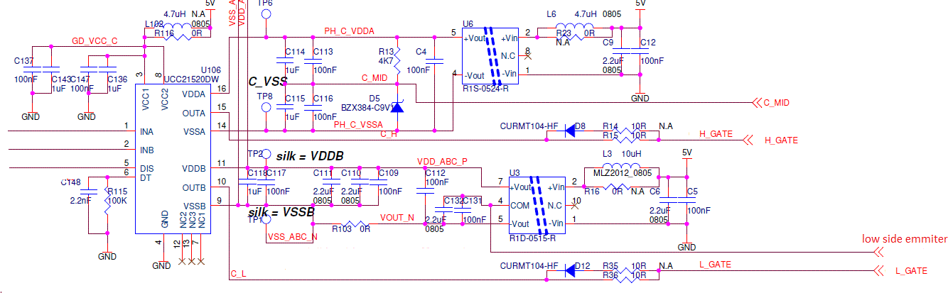
I use the UCC21520 to drive an IGBT which has 4.4nF input capacitance, 10 Ohm Integrated Gate resistor.

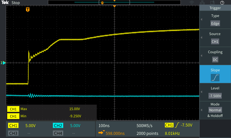
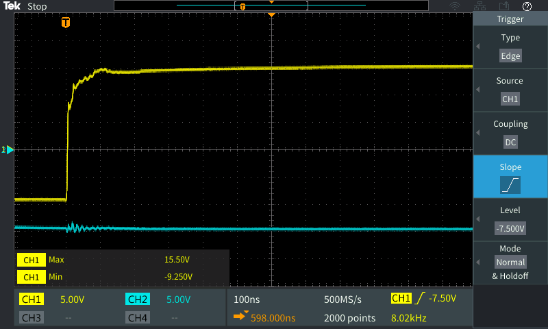
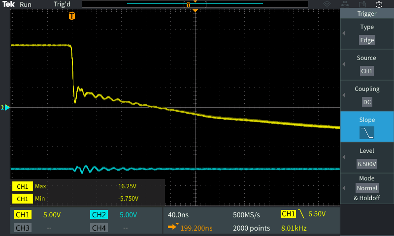
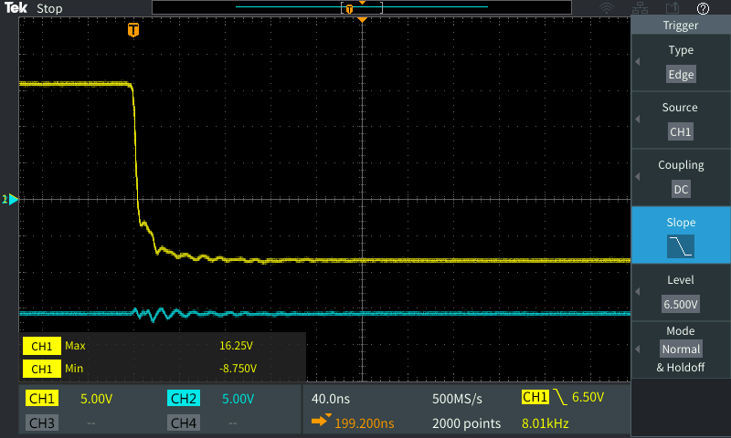
I used 7.5 to 10 ohm serial reistor to directly drive the IGBT gate. I observe that only when I use 0R (ZERO!) resistor, I get satisfying Switch- ON waveform (20nSec). The turn off waveform is also improved at 0 Ohm resistor (5nSec).

The resistor slows down switch ON time to 100nS or more.  I ask whether a 0R resistor is still a correct design, without over-stressing the UCC21520.

I calculated my peak source and sink current, with resistor = 0R, and I am well below 2A, which looks fine to me. 

My design:

I don't have  a bootrap diode. My VDDA cap is 0.1uF , VDDB cap is 0.1uF and 1uF.   

VCC is 5V, VDDA and VSSA is 16v and -9v while VDDB and VSSB is 16v and -16v, respectively.

No Rgs resistor.

Thanks for your support!

  • Hi Haggai,

    Thank you for your question. I work on the applications team in the high power drivers group.

    Since you are using an IGBT with a larger integrated gate resistor, it is likely acceptable to use a 0 Ohm resistor. These switching time goals do seem a bit fast for an IGBT. Is this the desired rise and fall time of the collector-to-emitter, or gate-to-emitter?

    The peak current of <2A should be fine, our device is capable of sourcing 4A and sinking 6A. What is your switching frequency? It is important to ensure that the device is not dissipating too much energy.

    Can you share more about your design, perhaps design schematics? The VDDA-VSSA voltage sounds fine +16V to -9V (25V). However, the VDDB-VSSB voltage needs to be changed. The +16V to -16V bias is 32V from VDDB-VSSB. This is larger than the abs. max rating in the datasheet and is likely to cause damage to the driver which could cause larger amounts of damage in the system. I recommend changing your CHB negative bias to -9V, to match the CHA supply. How is this supply generated?

    If this answered your question, could you please press the green button? If not, please feel free to ask more questions.

    Thanks and best regards,

    John

  • Dear John

    I am thankful for your helpful and quick response.

    I referred to the timings of the Gate to Emitter pulse. 

    IGBT's Gate emitter threshold voltage is around 6v

    Please see switching ON and then OFF, looking at the Vgs, WITH 10 Ohm resistor, and WITHOUT it: (scale: 5v and  40 or 100nSec per grid)

    My switching frquency is 8KHz.

    I am enclosing my schematics here as well. True, my CHB VDD-VSS is 32v and I will change that. My current dual output power supply of +\- 15v (See enclosed file. not regulated Recom's 1Watt module) may be replaced to +\- 12v, so it should be ok . It will NOT be same as for CHA though. Do you see any problem with that?

    Another solution that I can easily make on my PCB, is to still use the +\- 15v dual output power supply, BUT adding a 5 to 8 volt LDO on the lower rail. This way I can get +16v and -9v as well. What is your opinion?

    NEW INPUT...:  I reduced my external gate resistor to 0R and one of my gate drivers burnt after a short while. If I calculate max peak current, assuming 10 ohm internal gate resistor at the IGBT, to be 3.2A (i=32v/10R), then I am surprised.. Please assist me here?

    Many thanks

    Haggai

  • Hi Haggai,

    Typically, gate resistors are sized to limit high frequency ringing on the gates. The rise and fall time of the collector-to-emitter waveform is not entirely dependent on the speed of the gate-to-emitter waveform. I might recommend keeping some gate resistance, at least for the turn-on path. Can you share your IGBT part number, so I can take a quick look at it?

    Your proposed solution of using an LDO after the power supply is acceptable for dropping this VDD-VSS voltage. +16V and -9V should be good, as long as they don’t vary too much and violate the abs. max.

    On your update about one of the drivers being damaged:

    Which channel was damaged? Was it the one that still has 32V from VDD-VSS? If it still has this voltage, the damage is to be expected, since the output stage only has 30V FETs internally. You will need to reduce the VDD-VSS voltage and replace the part before doing any more testing.

    The driver should not be damaged by a large peak current alone. The output structure limits the output current based on the saturation characteristics of the internal FETs, and should not be damaged as long as they are driving capacitive loads and stay within the power dissipation limits of the device.

    Thanks and best regards,

    John

  • Dear John,

    Thanks for your reply.

    10 ohm opens the IGBT slowly - some 

    I use vincotech's V23990-P820-F10-PM (historic decision... not mine :-) )

  • Hi

    (message was sent before completion...)

    I wanted to point again to the fact that with a 10R resistor, the Switch ON took approx 140nS to reach the threshold switching voltage, and much more time to completely get the IGBT into saturation... 

    I will try the LDO solution, it is marginal though... A +/-15 power supply minus my 5v LDO brings me to 25v. It is common to get 32v from the power supply, though, so I am at 27v with this solution... How bad is it? (I do try to look for a 8 or 9 volt LDO with same footprint, no sucess at the moment...)

    best regards,

    Haggai

  • Hi Haggai,

    From the datasheet for this particular IGBT module, it appears that they recommend 4 Ohms for Rgoff and Rgon. I do see your point that it takes awhile to switch with 10 Ohms gate resistance, but this is still a fairly fast rise time when compared to the entire period/frequency (125us/8kHz). Considering this switching frequency, I would think that switching losses are still minimal. Do you have any waveforms showing the collector-to-emitter voltage, when switching with a load?

    What is the topology of this converter?

    We do not guarantee the specs from the electrical characteristics and switching characteristics tables when operating above the recommended max of 25V. Operating between recommended max and abs max won’t cause damage, but we don’t recommend it. Depending on your layout and load, you might be able to use a lower negative voltage, which might make your LDO search a bit easier.

    Feel free to read through the document below to learn more about how to interpret these specs.

    http://www.ti.com/lit/an/szza036c/szza036c.pdf

    Thanks and best regards,

    John

  • Hi John

    My concern about the slow "openning" of the IGBT, is not related to the overall time of the cycle.

    I am more concerned about the duation when the IGBT is "semi open". I am affraid tha the energy wasted on the transition time, between cut-off and saturation state, causes the IGBT to heat up. What do you say?

    I do not have Vce waveforms at the moment

    What do you mean with your question: "What is the topology of this converter?" 

    I use the IGBT to drive a motor (not sute "Delta" or "star")

    Regards

    Haggai

  • Hi Haggai,

    I understand your concern about the overlap between Vce and Ice switching losses. Gate resistance should be selected such that it damps the LC-tank circuit formed by the gate capacitance and drive loop inductance. The most efficient gate drive circuits will minimize this loop inductance, so as to minimize the size of the gate resistor. Please read through this app note to learn more about sizing your gate resistor.

    http://www.tij.co.jp/jp/lit/an/slla385/slla385.pdf

    This app note can help you with estimating the power loss in your IGBTs, since they share the same equations as MOSFETs.

    http://www.ti.com/lit/an/slpa009a/slpa009a.pdf

    I see that this is a motor drive circuit then. Have you had any success with lowering the VDD-VSS voltage and testing more?

    Thanks and best regards,

    John