


Hi Team,
I found that the function block is different between datasheet and EVM user's guide as picture below.
1. So which one is correct?
2. The truth table in datasheet is correct or not?
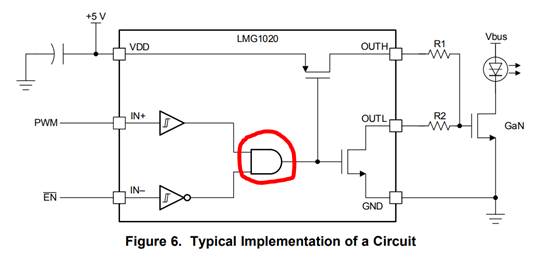
Thank you very much,
C.T.
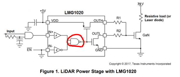
Hi Team,
I found that the function block is different between datasheet and EVM user's guide as picture below.
1. So which one is correct?
2. The truth table in datasheet is correct or not?
Thank you very much,
C.T.
