Hello,
I have designed a Buck connverter with the TPS92691 driver.
Vin = +18V to +26Vdc, Vnom = +24Vdc
Vo = 5Vdc (that is the Vf tipycal led value used as a load)
Io = +4.5Adc.
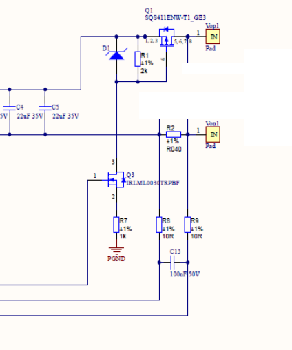
My doubt is about the correct values for Rls2, Rls1 and the zener diode used in the output stage of the converter. (Schematic R1, D1 and R7).
The datasheet only describes that this values can modify the time raise and fall for when a P-FET is used, which is my case. The schematic is as it is described in page 18.
The zener diode is used in the examples described in the datasheet.
I know that this is a bit dependant of the mosfet selected, but what is exactly the goal of this network to desing the adequate values? What's the correct way to design this network?
Another thing that I want to know is if that can produce a change in the output current when pwm dimming frequency is changed.
I mean, if and improper design of this network can produce this issue.
As far as I know changes in pwm dimming frequency should not change the output current value, only the duty cycle would produce it.
Regards,