This thread has been locked.

If you have a related question, please click the "Ask a related question" button in the top right corner. The newly created question will be automatically linked to this question.

BQ24170: TI EVM not passing EMC, need assistance selecting values for BTST and snubber C11/R12

Part Number: BQ24170

Hello,

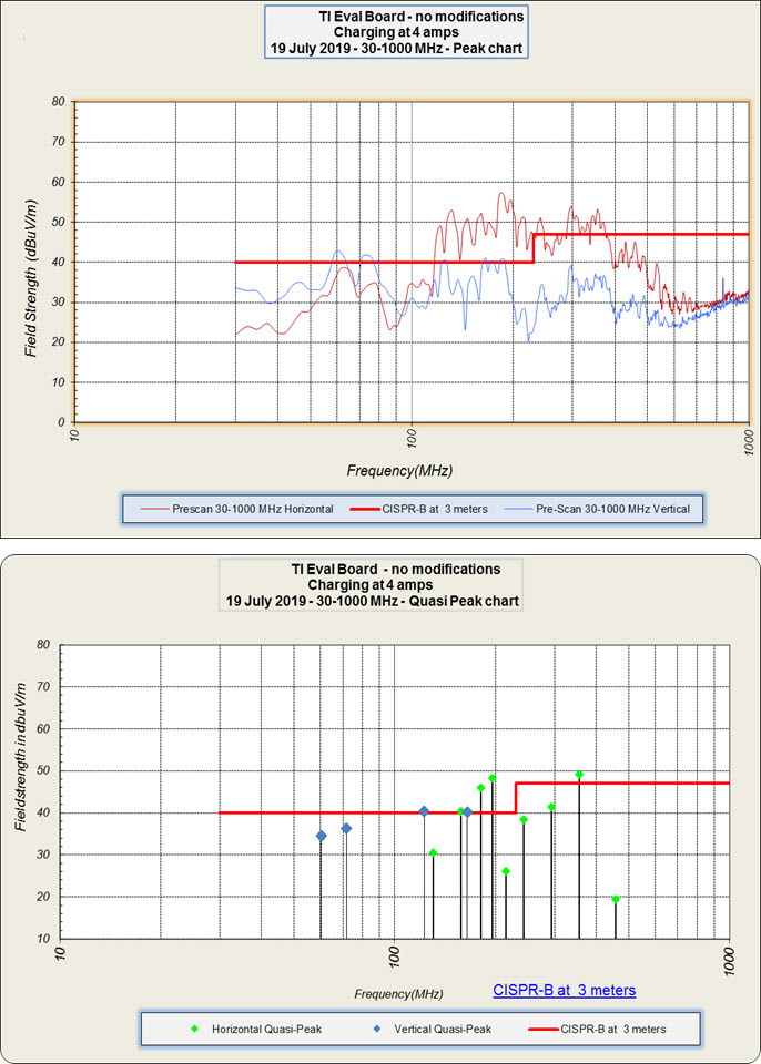
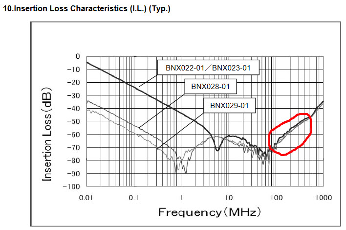
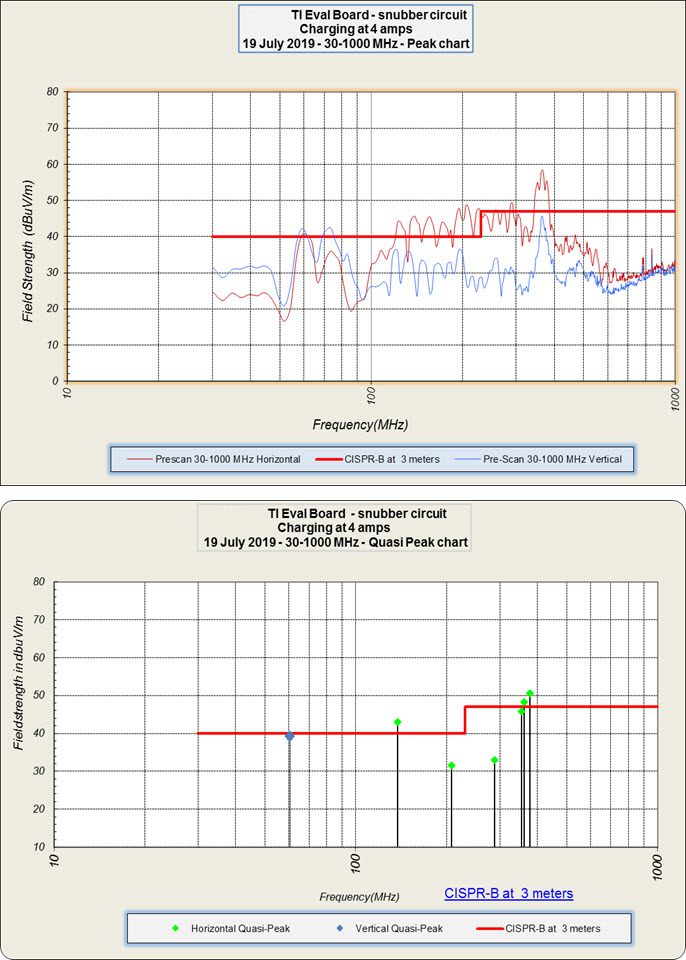
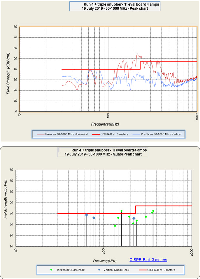
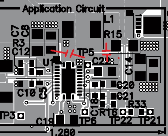
I have a customer whose design uses the BQ24170 and when enabled is caused EMC issues.  When comparing the EMC test resuts to those of the EVM by itself you can see they both fail in the same frequencies with the dominate fail at the Fsw ~1.6MHz.  The EVM has places for BTST and snubber but we are looking for guidance on what values to use in TI EVM to reduce the radiation so that a similar solution can be used on the customer design.  Please advise.

Tony

  • Hi Tony,

    Most EMC/I specs of which I am aware (FCC, CISPR) are at much higher frequencies than 1.6MHz, which is the charger's switching frequency.  We can't damp the 1.6MHz with an RC snubber without effectively killing the buck converter's operation.  If the 1.6MHz sensitivity is specific to their application, then we might be able to find a different charger that operates at a different frequency or move to a linear charger. Alternatively, they can use a metal shield like cell phones do.  If the EMC/I issues are at much higher harmonics (100MHz+) of the 1.6MHz, then we can use the procedure below. 

    First, when making the measurement on the EVM or their board, make sure all headers and test points on power inputs and outputs that could be antennas are removed.  Then make sure that the input power to the board is either from a non-switching or heavily shielded power supply with a short cable to the input.  Otherwise the input cable or supply will generate the noise. In the past I have used a 12V/6V battery + LDO to generate input power.   

    If test setup is resolved, then the next step before snubber is using input and output decoupling capacitors (0.01-0.1uF) close to IC PVCC and BAT and GND pins.   If that doesn't work, then we add a BTST resistor (~3-5ohm) and start looking at the SW/PH noise for ringing and use that to size the snubber components. There are several appnotes on the web about how to size a switching converter RC snubber.  I wrote a very simple one for a boost converter but the principles are the same for a buck converter.  http://www.ti.com/lit/an/slva255/slva255.pdf   The procedure requires using a high bandwidth (400MHz+) oscope with voltage probe having short ground return cable to measure the ringing at the SW/PH rising/falling edges.  Then based on the frequency of the ringing, size the snubber to damp it. 

    Regards,

    Jeff

  • Thanks for the thorough response Jeff.  yes, we are aware that the fundamental freq is not the offender here but the fast transients and associated ringing is whats likely the culprit so we need to filter/slow that down.  Given the unique customer design the specific values in that system will depend on many factors but in this case we were hoping to get those values that work for our EVM as-is and reduce the experimentation.

    The customer is currently exploring these options but open to more specific values if you have them.  In addition, they will explore the shielding recommendations, so far FB's have not resulted in any improvement.

    Another related question to the EVM is the function of the Schottky Diode (D2) in a synchronous design.  Is it there to deal with the transient between high-side and low-side FET transition?  Is the FET body diode not adequate to handle this?  You can remove D2 with minimal impact on switching waveform but perhaps doing so risks the long term reliability for the device?  Please advise.

  • Hi Jeff,

    This is customer Lance.  Thanks to you and Tony for the help,  much appreciated.

    I want to emphasize that right now,  we are simply trying to make the TI eval board BQ24170EVM-610-15V (EVM) pass EMI testing. 

    Why are we testing the TI EVM?  Our own board using this part is failing, we identified conclusively it is due to harmonics of the BQ24170 1.6MHz switching frequency. Before spending effort adjusting our board layout we want to know that its possible for this part to pass and we want to know what key ingredients are required.  We figure the TI EVM,  with a close to ideal layout (one of the key ingredients),  it the right vehicle for this "prove it can work" test.

    So the discussion in this thread should be entirely about the TI EVM.  If we can make it work/pass EMI then we can proceed with our own board re-layout with confidence.  This is our thought process.

    In all our EMI testing the EVM is configured to charge a 2-cell approx 10AH Lithium battery at 4A.  All tests are run while charging a mostly-discharged battery (ie: BQ24170 is in constant current charging state).  Cable to battery is about 4".  We verified that the input voltage (from a regulated power supply) is solid/stable - no funny oscillations or ringing).

    Out-of-the-box,  the EVM with only the one modification to increase charging current to 4A fails EMI:

    You can see the failing frequencies are all between 100-400MHz.  If we zoom-in real time on any of these frequencies we see a comb of small peaks separated by the 1.6MHz switching frequency, so it's entirely clear the failing frequencies are related to the BQ24170 switching.

    NOTE:  Interpretation of the EMI plots:

    • Top plot is peak measurement.  Being above the pass/fail line does not necessarily mean EMI test failed.  The top plot is useful for comparing one scan to another to get a quick general idea of differences.
    • Bottom plot is the definitive pass/fail measurement.  Worst case frequencies from the top plot are selected for quasi-peak measurements which are displayed in the bottom plot.  If these select frequencies are above the limit then the test fails.

    By the way,  the above results are remarkably similar to EMI results for our own board,  which has a very different layout than the TI EVM.  This makes us think there must be some fundamental thing going on with the BQ24170 that can't be resolved by simply improving our own board's layout to be more ideal.

    To answer the question about the input/output cables to the EVM radiating like antennas,  we reworked one of the EVMs (we purchased several) to add really good common mode chokes on both the input and output sides - input/output cables were connected directly to the chokes.  Choke PN is Murata BNX022-01L which has very good attenuation in 100-400MHz region:

    Use of the chokes did not make much difference at all in EMI - maybe subtle difference in shape of peak measurements (top plot) but still have plenty of failing frequencies measured quasi-peak (bottom plot):

    Conclusion:  Adding EMI chokes to kill emissions radiating from cables had almost no effect.  Therefore the EVM EMI issues are not related to input/output cabling.  By the way I have lots of other EMI near-field sniffing data indicating that the EVM EMI issues are not the cables radiating.  In fact it really looks like the entire EVM board is acting like one big radiator.

    We did some quick experiments with BTST resistor,  this really didn't have any effect.

    Jeff you had suggested shielding as something to try.  We considered this but doing so on the EVM looked impractical.  To put an effective shield down one needs to tie it to a common ground all around the periphery of the shield.  The TI EVM has two different ground domains (analog GND and power GND),  and there is really no way to draw a line around the EVM circuitry and tack a shield down to just one of the grounds all the way around.  Plus there are many other signal pour areas around the circuitry that are not ground:

    We think to add an effective shield we'd have to design a custom board with appropriate "ring of vias" into just one of the ground domains all the way around the circuitry area,  so that the shield could connect into the one ground domain through the vias (maybe I should call them through holes).  Since we are trying to make the existing TI eval board work we abandoned the idea of experimenting with shield for now... 

    Next we tried adding a snubber according to the design procedure in this white paper: http://www.ti.com/lit/an/slyt465/slyt465.pdf (which I think is the same procedure called out in the app note you referenced).  We measured the ringing frequency in the EVM to be 180MHz and following the design procedure ended up with subber components of 680pF and 3.75 ohms.  Adding these snubber components to the EVM did very effectively remove the 180MHz ringing from the switching signal when viewed on an oscilloscope (1.5GHz scope using 1GHz very low capacitance active probe),  but did not solve all of the EMI problems.  Here's the EMI scan with snubber installed:

    You can see in the above plot that in fact the snubber did push things down in the ~180MHz region,  but did not help at lower frequencies and seems like it pushed 300-400MHz range up a bit (I've seen this before with snubbers effectively hitting the frequency they are designed for but then pushing up at other frequencies).  None of this is surprising because the snubber in this case was designed to suppress just the single 180MHz ringing frequency,  not the broad swath of frequencies being emitted by the EVM board.

    As a quick experiment we "tripled" the snubber:  three 680pF caps in parallel and three 3.75 ohm resistors in parallel.  This doesn't change the snubber's corner frequency but definitely pulls more energy away from the switching node at frequencies above the snubber corner frequency.  Purpose was to see if we could squash the 300-400MHz frequencies,  and we did:

    So it seems the TI EVM requires snubber to control EMI. 

    But from the above plot you can see the TI EVM still has problems below 180MHz even with the triple snubber (C=2040pF, R=1.25).

    We think our next step should be to increase the triple snubber capacitance to lower the corner frequency down to about 120MHz.  This would mean a snubber circuit with about 3000 pF and 1.25 ohms.

    We haven't tested this yet but would really like to have your opinion about these component values and their appropriateness for the BQ24170 (and the EVM board EMI situation) especially when running at the maximum 4A charging current.  Please comment, thanks!

    Bottom line is that we think "strong snubbing" is the way to make the TI EVM board pass EMI.  We are hoping to get a sanity check from you/TI that this indeed is the general trend you see among your customers for the BQ24170 part - that it generally requires a snubber.  Having this indication from you will help us gain confidence that we can make the part work successfully in our own board.

    Thanks very much for your help!

    Lance

  • Hi Jeff,

    This is the customer Tony mentions,  Lance.

    Thanks for your help!

    EDIT:  After submitting the first reply above,  I received no confirmation nor any pop-up notification of error or anything.  So it seemed my reply, which I'd spent a couple hours putting together, might have gone into a black hole.  I was pretty disappointed at that moment...  Subsequently I've come to realize that the replies go through moderation check before posting to the website, so now I know there is no black hole.  But it was startling as a first time user.  Would be great if you could forward a suggestion to your web master to have a simple line of text above/below the Reply button indicating all replies go through moderation with some delay before posting.   Anyway,  after thinking I'd lost my first post I wrote up the summary below,  along with a list of specific questions.  I'll let the summary remain because it might be helpful.  Please do look through the list of specific questions and I hope you can provide feedback on all.  Thanks!

    FURTHER EDIT:  I've seen in a subsequent post a very brief pop-up notification about moderation of the posts.  This pop-up did not appear on my very first post and that's why I was startled.  My suggestion remains:  add some simple text near the reply button so there is no doubt in the user's mind that there will be a delay.

    Here is the restated summary of previous post: 

    We are currently trying to make the TI BQ24170 EVM board pass EMI testing in order to prove it is possible for the BQ24170  part to pass,  before we execute re-layout to our own board (which has BQ24170) to try and make it pass EMI.  Don't want to waste time re-laying out our board for this part if we can't figure out how to make the optimum-layout TI EVM board pass...

    We verified conclusively that the TI BQ24170 EVM board can't pass EMI out of the box (only modification is to increase charging current to 4A for 2cell battery).  We absolutely confirmed good power supply signal going into the board, verified radiation from cabling isn't the issue (adding common mode chokes to both input and output sides didn't change EMI results at all). All failing frequencies are related to "combs" of 1.6MHz harmonics of the BQ24170 switching frequency.

    Adding a shield is impractical.  If you look at EVM board top side copper and try to trace a path to lay the shield down around the circuitry you will see that the shield passes over a number of different signal pours,  and two different ground domains.  No way to effectively tie the shield down to a single/common ground domain all the way around which is what one needs for good shielding.  So we didn't even try this.

    We played with BTST resistor, didn't have much effect at all.

    In the end we found a snubber to be effective.  The design procedure in the app note produced a snubber with 680pF and 3.75 ohms,  and this did effectively kill the 180MHz ringing in the switching signal.  But the EVM board fails across a broad spectrum of frequencies from 100-400MHz.  We "tripled" the snubber to about 2000pF and 1.5 ohms - this was effective at squashing all the frequencies above 180MHz but it still fails a few frequencies in 100-160MHz range.

    So now we're thinking to reduce the corner frequency of the snubber by increasing the C to about 3000pF and keep the R at 1.5 ohms.

    Questions to you:

    1. Does C=3000pF and R=1.5 ohms seem reasonable for a snubber on this part running at 4A? The EVM board gets pretty warm even without snubber and I just want to be sure that we're not going to push the part too hard by adding a strong snubber.
    2. Can you confirm or even just hint whether adding a snubber is the general trend that TI customers have had to employ with this part to get it to pass EMI testing?
    3. Anything else we should be looking at to make the EVM board pass EMI?  Remember we are doing this experiment as "proof of concept" that it is possible to make the BQ24170 work with a good layout,  and so far we still haven't successfully crossed that finish line.
    4. Tony asked in his reply below about the Schottky Diode (D2).  This question comes from us.  It doesn't make any sense why an external diode is required for a synchronous regulator part like BQ24170 yet there it is on the eval board with no explanation why.  The diode shows up also in the datasheet reference schematic yet there is no explanation of its purpose in the datasheet.  We removed the diode on the TI EVM board and didn't observe any real change in it's operation nor did we observe any real change in the switching signal (used 1.5GHz scope with 1GHz low-capacitance active probe).  Therefore we are very puzzled about why it shows up on datasheet and eval board and we suspect it might not really be needed?  Please let us know about this diode.
    5. What is the minimum practical supply voltage to the BQ24170's PVCC (switching/power input)?  The datasheet specifies the analog power input AVCC must be 300mV over regulated battery voltage (in our case with two cells it is 300mV over 8.4V),  but the datasheet doesn't say anything about how much over the regulated battery voltage PVCC must be.  Please advise.

    Thanks much for your help on this!

    Lance

  • Lance,

    I apologize for you needing to double post. The forum has a staging area for new/large posts to be pre-screened to prevent spam.  Regarding the EMI for the EVM, we have never tested these particular EVMs for EMI.  In the past, we omitted the EMI reducing components in order to market the minimum components necessary for operation and maximum efficiency. 

    Regarding 1, that much capacitance on the SW/PH node will significantly reduce efficiency on any buck converter and is probably impractical.  The IC has thermal regulation so it will simply scale down the current to prevent damage.

    Regarding 2, I honestly don't know if most customers frequently require a snubber or not with this IC.  I only started supporting this product about 9 months ago and this is the first time I have been asked this question.  My predecessor didn't leave notes about EMI being a common question so I assume either it wasn't or most customers used a shield.

    Regarding 3, this older EVM has larger footprint capacitors and the inductor placed close to the IC.  I suggest adding 0.01-0.1uF decoupling capacitors as shown below and then a 5 ohm BTST resistor for R20.   Then go back and resize the snubber. 

    You might also add the same decoupling capacitors at the EVM terminal blocks for VCC and BAT.

    Regarding 4, the diode is used to increase efficiency.  The internal low side FET body diode turns on briefly during the dead time.  The external Schottky reduces the drop from 600mV to 300mV during that time. 

    Regarding 5, the datasheet reports the typical maximum duty cycle as 97%.  You can use the equation below to compute the minimum input voltage. 

    VPVCCmin = VBATmax/97% + ICHGmax x (RDSon-HSFET + DCR) 

    I hope this helps.  Please let me know if I can help further.

    Regards,

    Jeff

  • Hi Jeff,

    Thanks very much for the helpful answers and info.

    This is a tough one for us because we really want to gain some faith that the part, in a more "ideal" layout environment than our own current revision PCB, can actually operate under FCC limits of EMI.  This means we really want to see what it takes to make the eval board pass.  So far the only thing that's reduced EMI substantially is the snubber with ~2040pF and 1.25 ohms,  but there were still some lower frequencies failing and that's why we're inclined to lower the corner frequency of the snubber with a larger cap (tomorrow we're testing 3300pF and 1.25 ohms in the chamber).  I've tested this on my bench,  not for super-long periods, but it seemed to work OK.

    We're not worried about having the highest efficiency,  though would be worried if we're pushing the part too hard in terms of thermal dissipation.  So if we go with the "stiff" snubber then we will need to do some further analysis to understand the thermal implications.

    You've mentioned shielding a few times.  I've never had to shield a buck converter before and it would be difficult to experiment on the eval board for reasons outlined in my previous post - thus difficult to get any data about what shielding does before expending effort to try and wedge a shield into the next layout of our own board. So it's tough for us to be enthusiastic about shielding as a good path forward. But we're all ears if you have prior experience with shielding really helping this class of buck converter - please by all means try to sway us if there's good reason.

    Thanks for all the other info and suggestions - all helpful.  We may try throwing some additional caps onto the eval board tomorrow as you suggest,  and for sure will keep the Schottky diode in our own circuit.

    Best Regards,

    Lance

  • Lance,

    Placement of the input and output caps as close as possible to the IC is critical, even if you have to move the inductor further away.  Same for the RC snubber from SW to GND.  The additional caps at the EVM terminal blocks are more for reducing noise on cables in the test setup.  The resistor in series with BTST should change (hopefully reduce) the value of snubber components needed.

    I personally haven't used metal shielding so can't provide much advice there.  In theory, it should work but will require careful board layout.

    Regards,

    Jeff

  • Thanks Jeff,  I think we're good for now in terms of gathering all your thoughts & suggestions.  Appreciate the help!

    Lance