A related question is a question created from another question. When the related question is created, it will be automatically linked to the original question.
If you have a related question, please click the "Ask a related question" button in the top right corner. The newly created question will be automatically linked to this question.
Gordon is currently out for a few days, but I wanted to follow up with a few requests:
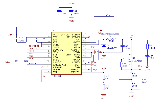
1) Can you confirm the values of the decoupling capacitors on pin 21 (output) and pin 27 (input)?
If they are reduced or not present it could explain the noise.
If they are present, please consider probing directly across the capacitor like the measurements for VBAT.
2) With the lead wire being used for the test point, please consider minimizing the loop area created by wire to the probe and the ground clip to the GND connection to reduce coupled switching noise.
While Gordon is on vacation, can you please explain your schematic to make sure you don't have two supplies tied together as it appears in the schematic capture. It looks like you have Pin 22, VDDIO tied to pin 21, VDD3/5 which is normal. VDD3/5 is normally used as the IO rail in a system and thus is common to be the IO supply (VDDIO) to the TPS65381A-Q1. However, on the attached image it is impossible to determine if that is tied into a net called 3.3V VCC which is tied to pin 20, VDD5 or it is actually two separate nets and the net symbols are just overlapping making it look like the nets are tied together. Pin 20 is VDD5 is a 5V LDO output and cannot be tied to VDD3/5.
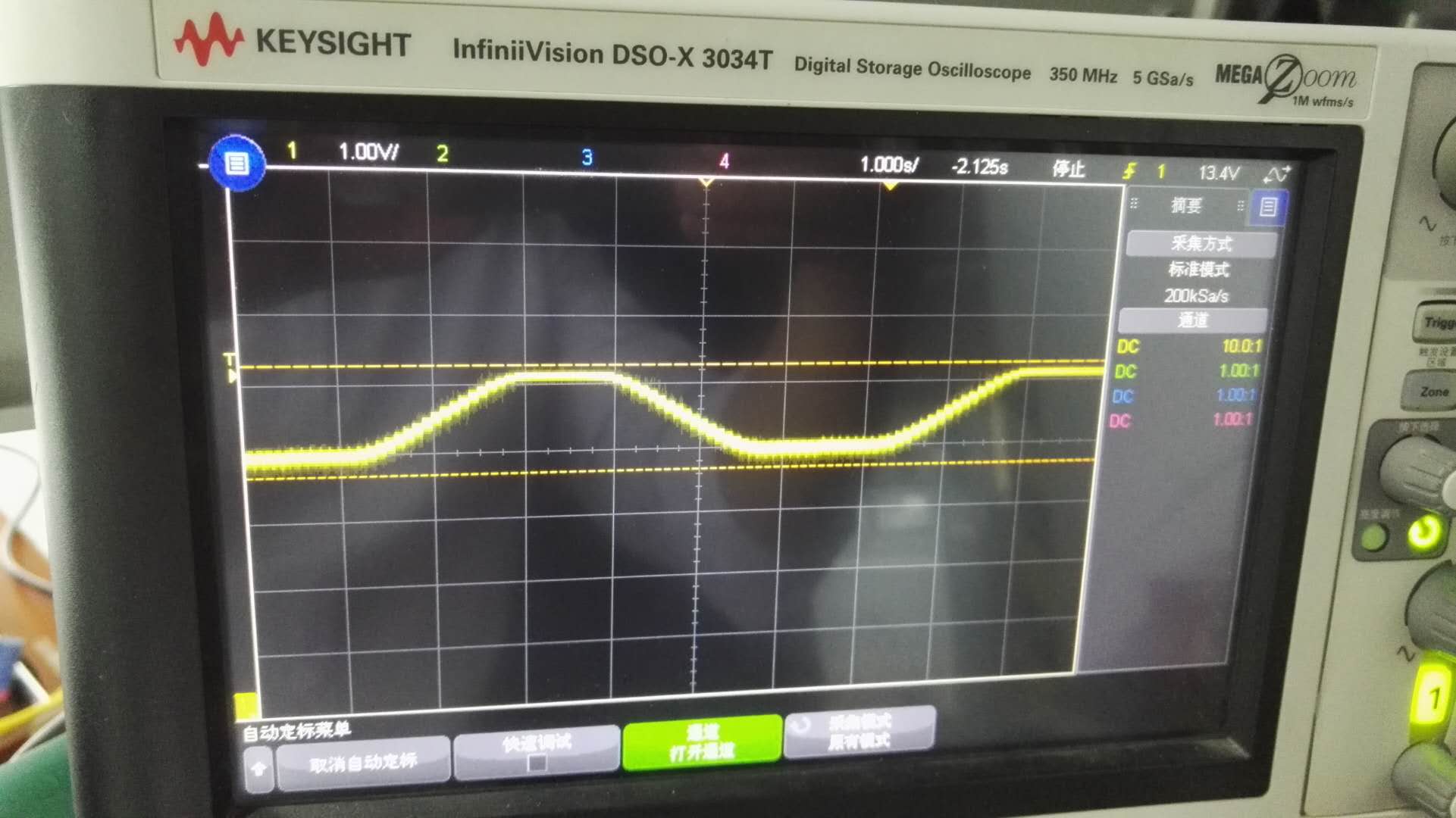
Can you please use all the channels on your scope and provide the a waveform with these signals present, triggered on the rising edge of IGN pin: IGN, VBATP, VDD6, VDD3/5. And a second plot with IGN, VCP, VBATP, NRES.