This thread has been locked.

If you have a related question, please click the "Ask a related question" button in the top right corner. The newly created question will be automatically linked to this question.

BQ40Z50-R2: writing data flash

Part Number: BQ40Z50-R2
Other Parts Discussed in Thread: BQ40Z50, BQSTUDIO

I am attempting to write to the BQ40z50 data flash (0x4000 - 0x5FFF) and have not been successful.  I've confirmed that the device is in "full access" mode by examining bits 8-9 of the OperationStatus() register, and also confirmed that a "permanent failure" has not occurred related to the data flash by examining the PFStatus() register (as 0x0000 is returned).

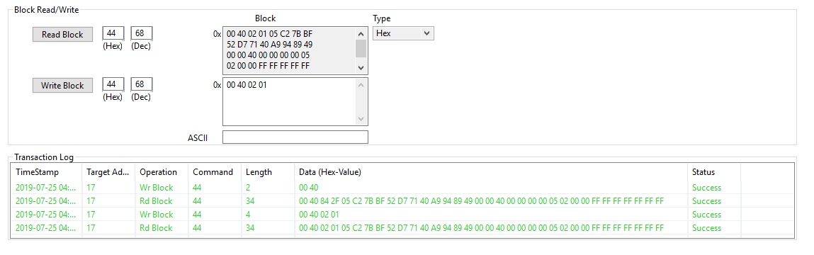
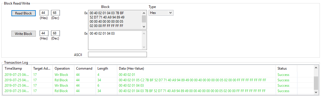
To write the data flash, I am sending the following I2C string:  0x44, 0x06, 0x00, 0x40, 0x01, 0x02, 0x03, 0x04

It is important to note that a PEC byte is not included.  I ave been successful in reading the data flash block starting at location 0x4000: The 32-byte data block read matches the default values found in the TRM.

Can you advise?

  • Hi David,

    The df doesn't incorporate any checksum or something for write verification, all you need to do is just follow the steps in the TRM to point to the correct location and then write the data. For this you need to be unsealed and have no PF, which you have already done. Also, please make sure that your voltage is greater than flash update voltage, a df parameter.

  • Hi Batt;

    They are pointing to the correct location and following the steps in the TRM.  Can you let me know what is wrong with the I2C wrtie they are trying?  0x44, 0x06, 0x00, 0x40, 0x01, 0x02, 0x03, 0x04

  • HI Batt;

    The voltage() smbus command is indicating a voltage of 8.09V which is greater than the "valid update voltage" (flash update) default value of 3500mV, we have a 2S battery system, so the voltage will be in the range of 6.8-8.4V.  Is this acceptable?

  • That is acceptable.

  • HI Batt;

    We have not been successful and I would like to get your specific answer to the question on the I2C command:

    1.  To write 0x4000 with data 1,2,3,4, Do you need the string length included? Is this command sequence correct?

     0x44, 0x06, 0x00, 0x40, 0x01, 0x02, 0x03, 0x04

    It does not seem to follow the TRM Write to DF example: Assuming: data1 locates at address 0x4000 and data2 locates at address 0x4002. Both data1 and data2 are U2 type. To update data1 and data2, send an SMBus block write with command = 0x44 block = starting address + DF data block = 0x00 + 0x40 + data1_LowByte + data1_HighByte + data2_LowByte + data2_HighByte

    Would this be the correct sequence: 

    {0x44, 0x00, 0x40, 0x01, 0x00, 0x02, 0x00, 0x03, 0x00, 0x04, 0x00}


    2. To resolve this, can you send me the correct write sequence and any other commands which are required prior to writing this sequence to the data flash?


  • Hi,

    It looks like the "Flash Update Voltage" is correct and the device is not sealed and no PFs, so the sequence should work.

    Using bqStudio on my bq40z50:

    Read of 0x4000, and writing 0x4000, 0x4001 to 0x0102:

    Write to 0x4000..0x4003 to 0x0102 and 0x0304:

    Read of data flash:

    The Data Flash values change as expected (0x102 hex = 258 dec, and 0x0304 hex = 772 dec)

    From a I2C controller, you will have to provide the length after the address, and typically it will be {0x0B, 0x07, 0x44, 0x00, 0x40, 0x02, 0x01, 0x04, 0x03}

    Can you try it with bqStudio to see if it works? then you can use a I2C bus monitor or logic analyzer to duplicate from there.

    Regards,

    Swami

  • But won't  {0x0B, 0x07, 0x44, 0x00, 0x40, 0x02, 0x01, 0x04, 0x03} be interpreted as the AtRateOk SBS command?   0x07 AtRateOK()

  • We don't explicitly specify the length, but when I monitor it using a bus sniffer, I can see the SMBus address, and the length of the data (in this case 0x07), and then the data as shown above.

    You can see the exact sequence followed in bqStudio in the first two images.

    Regards,

    Swami