This thread has been locked.

If you have a related question, please click the "Ask a related question" button in the top right corner. The newly created question will be automatically linked to this question.

TPS55340: Wrong Boost output depending on the enable pin

Part Number: TPS55340

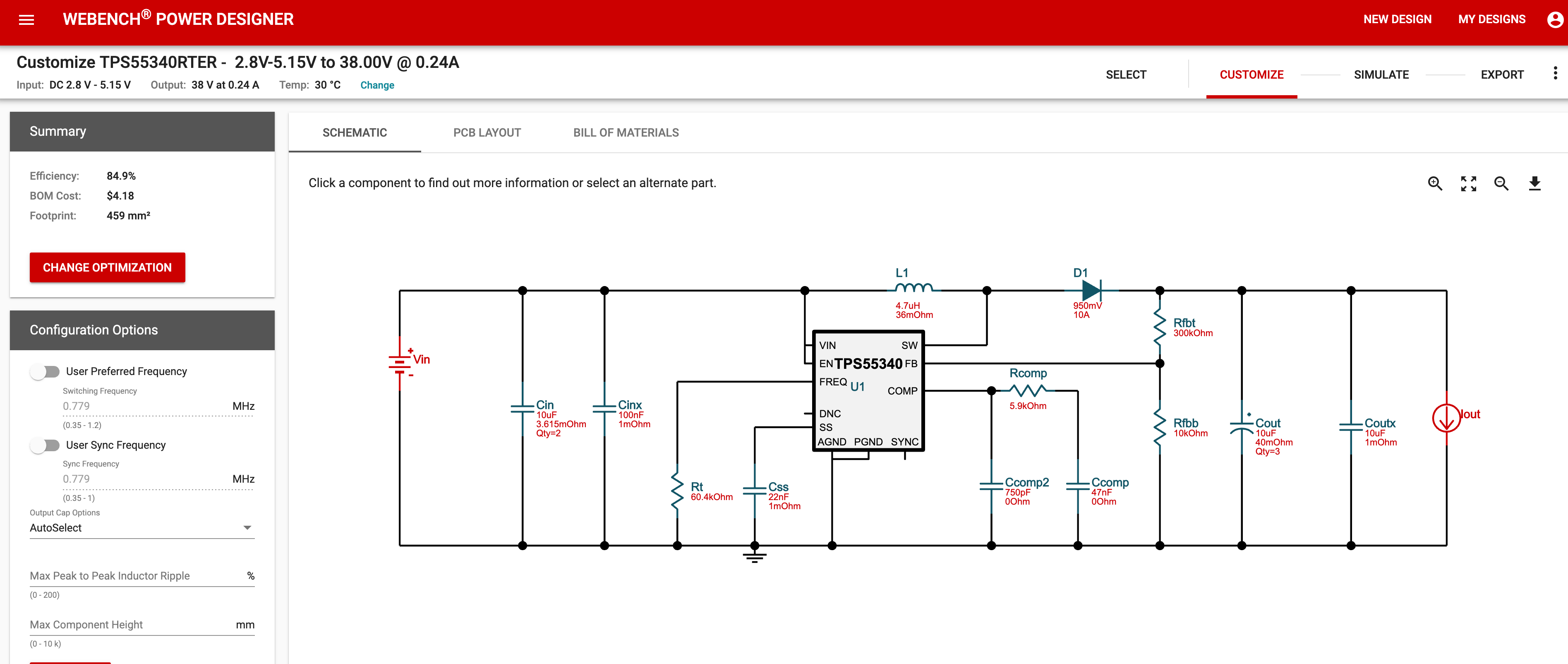
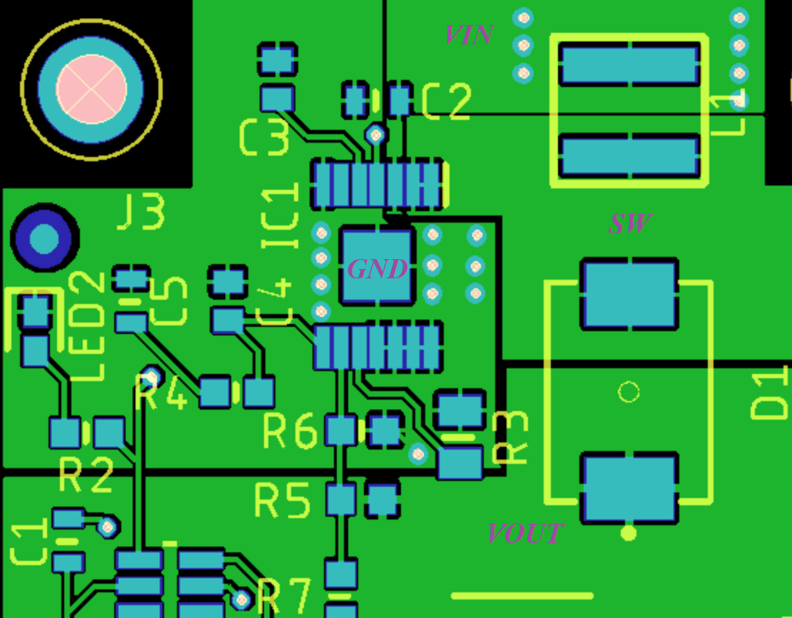
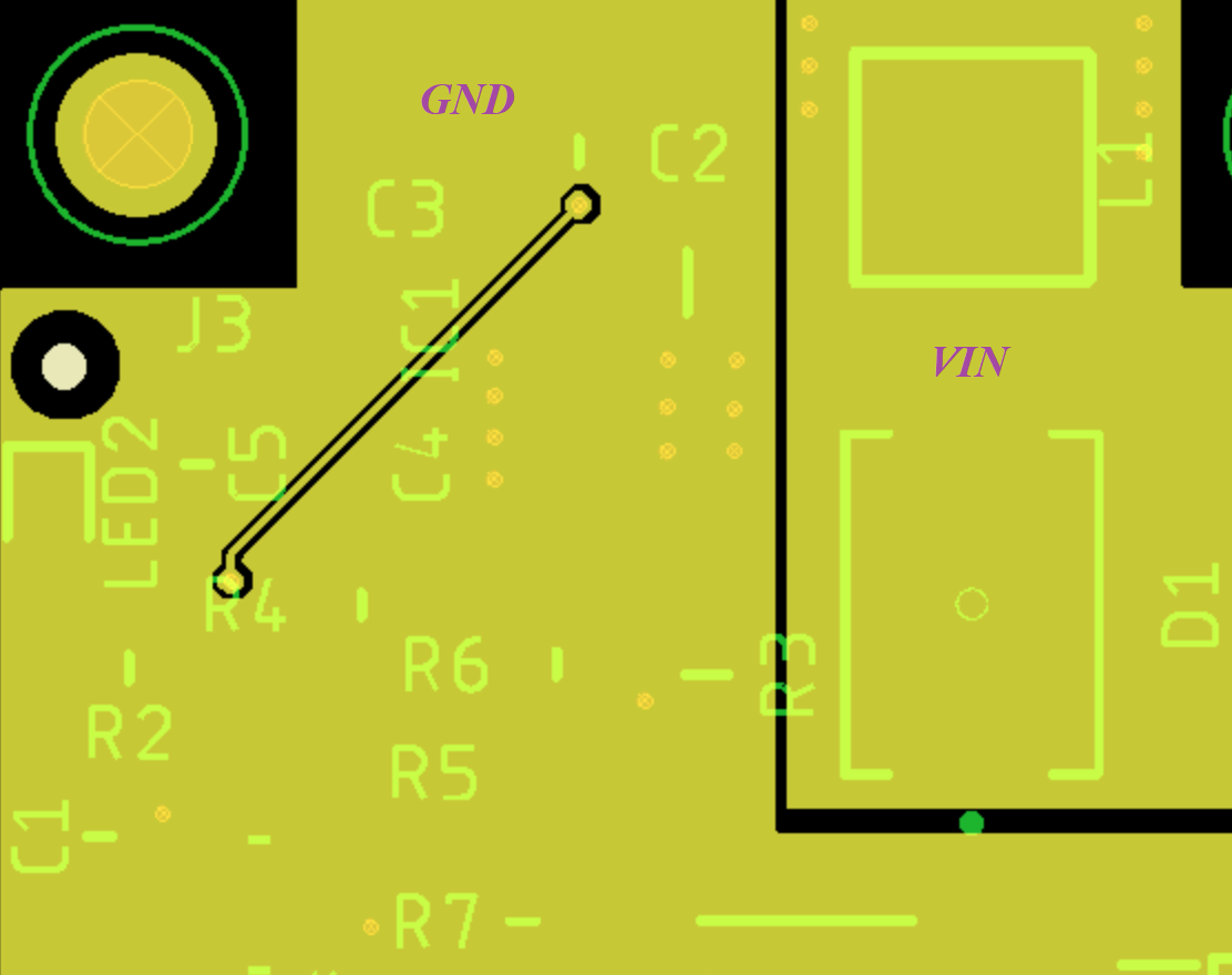
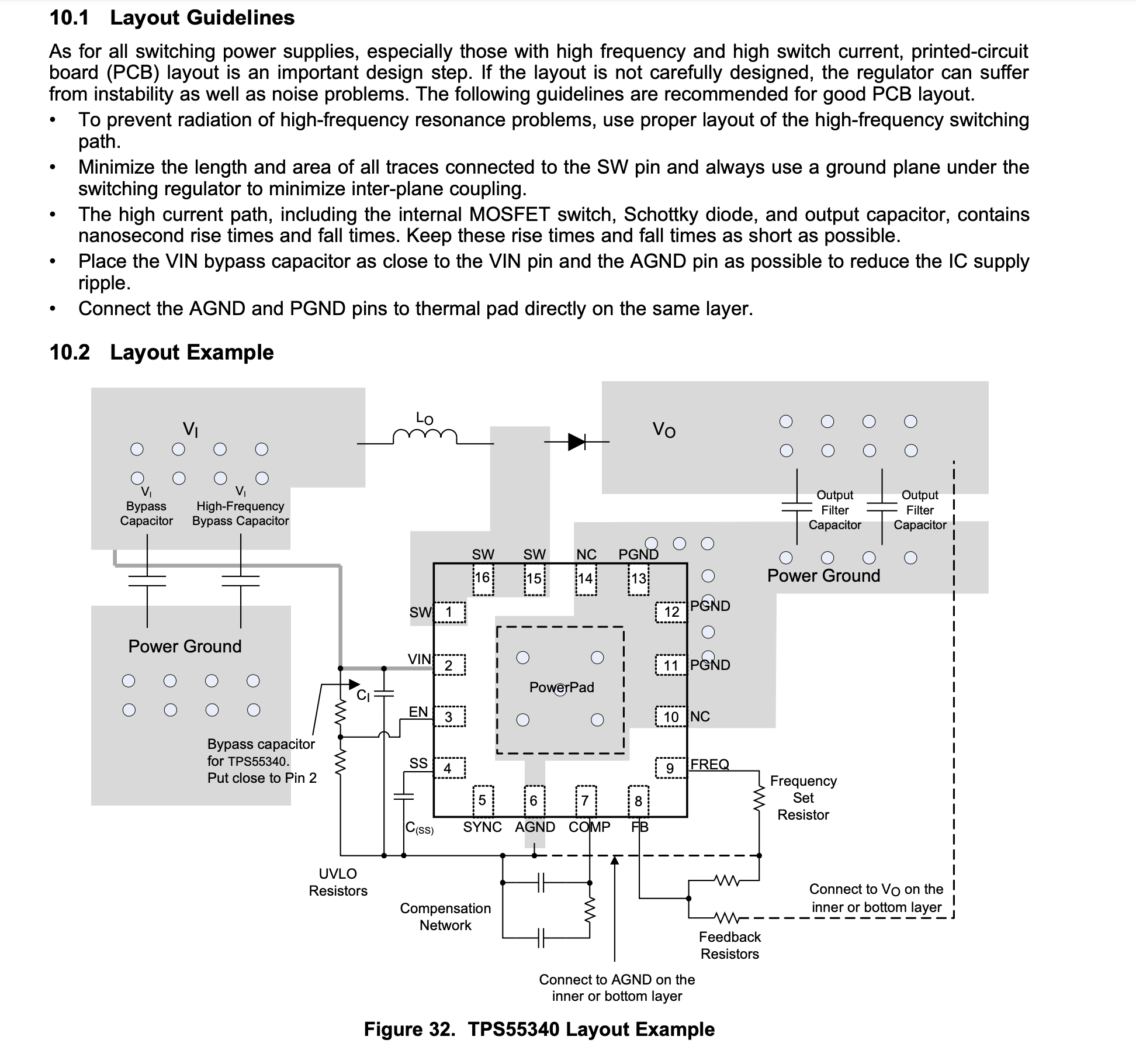
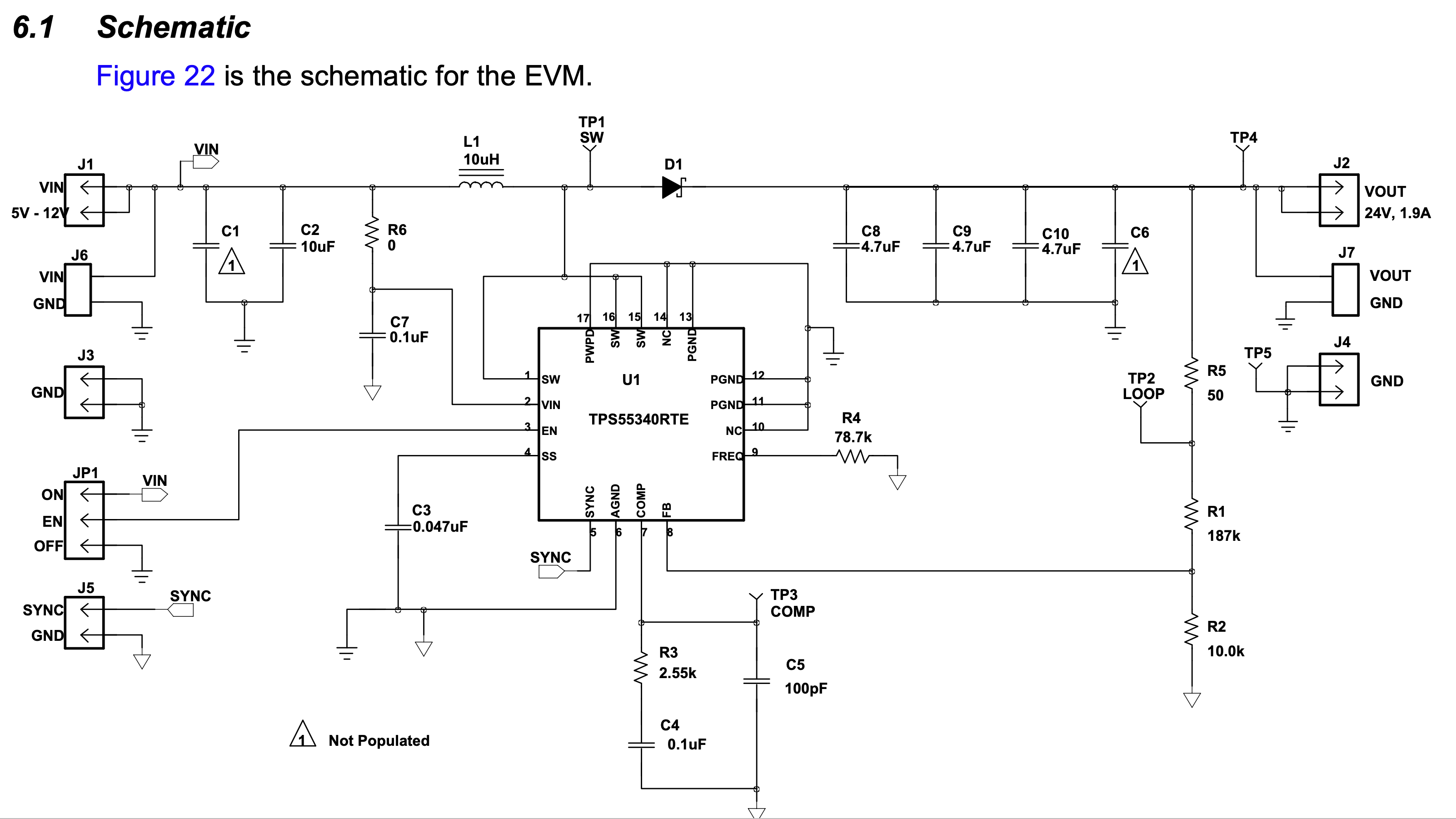
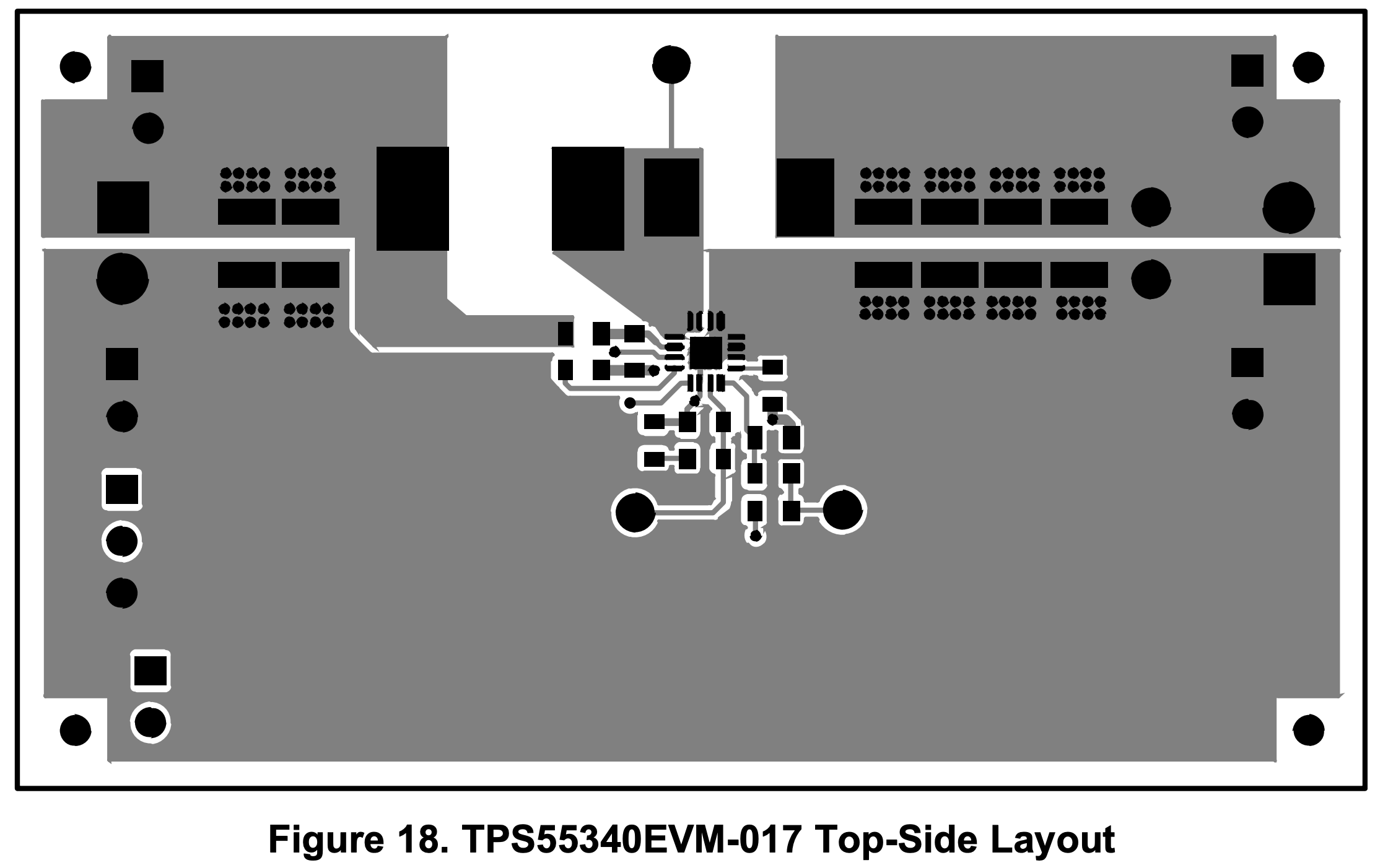
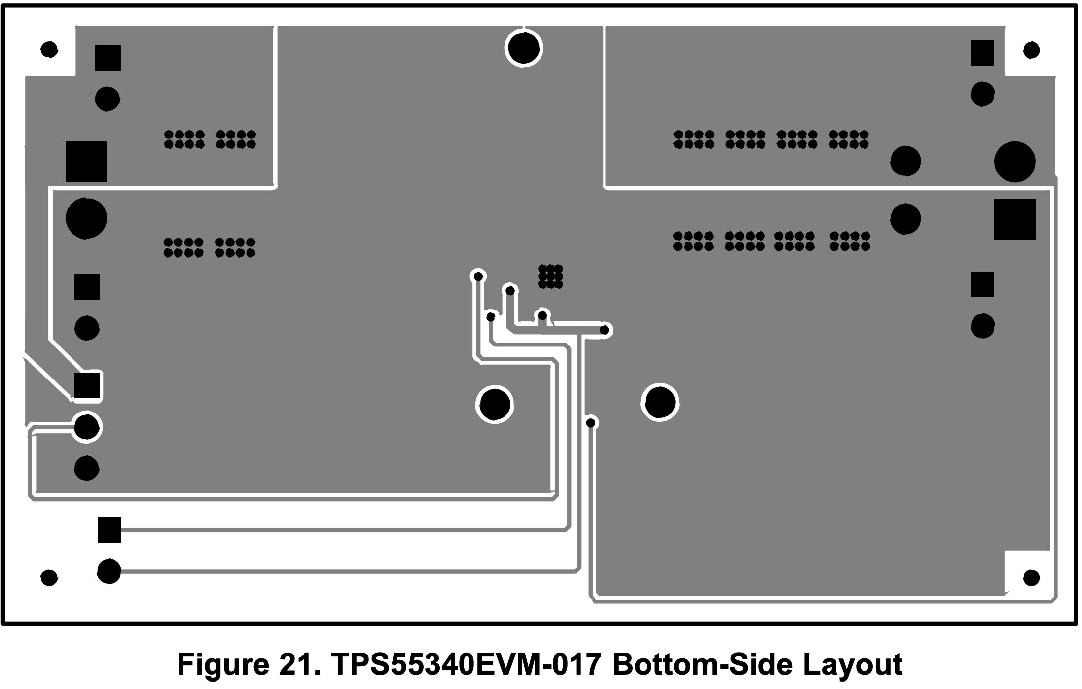
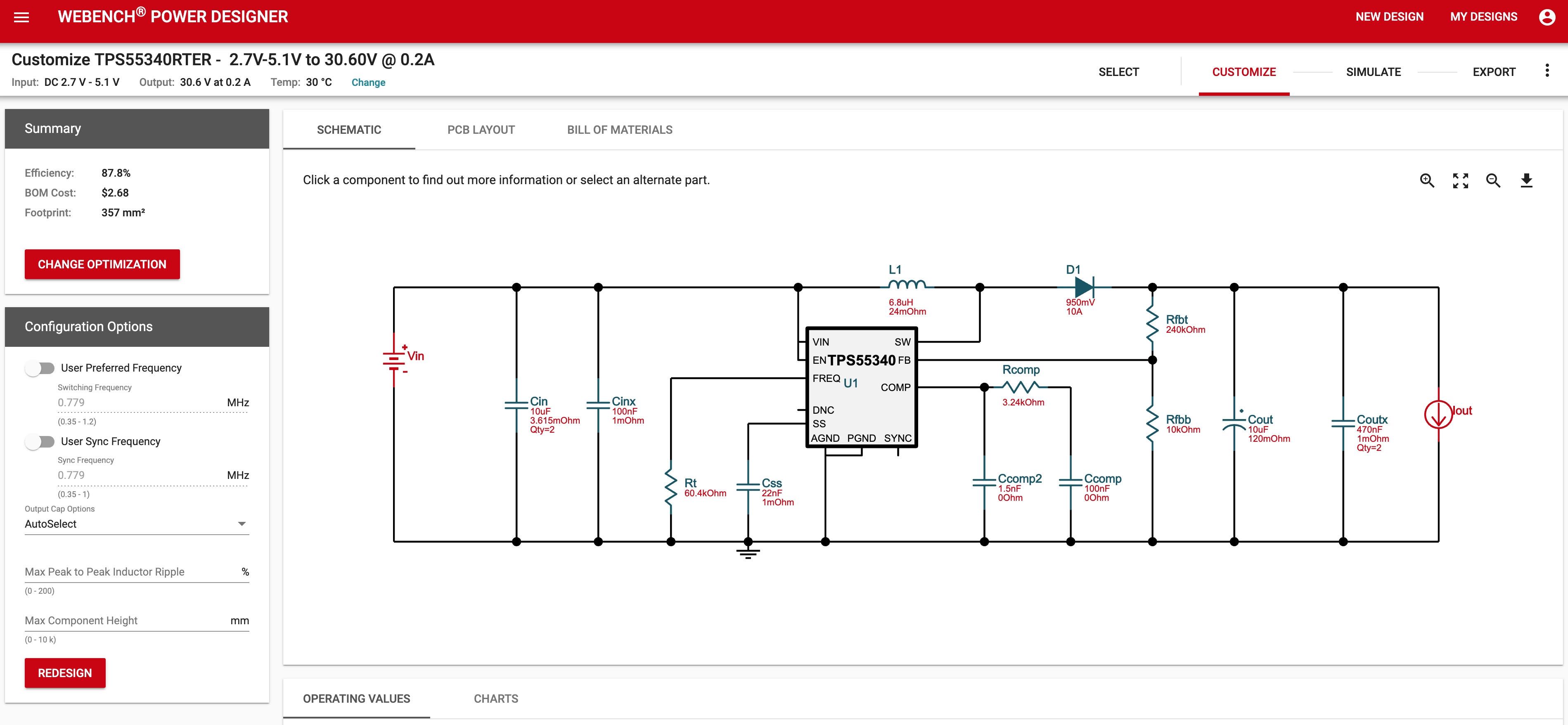
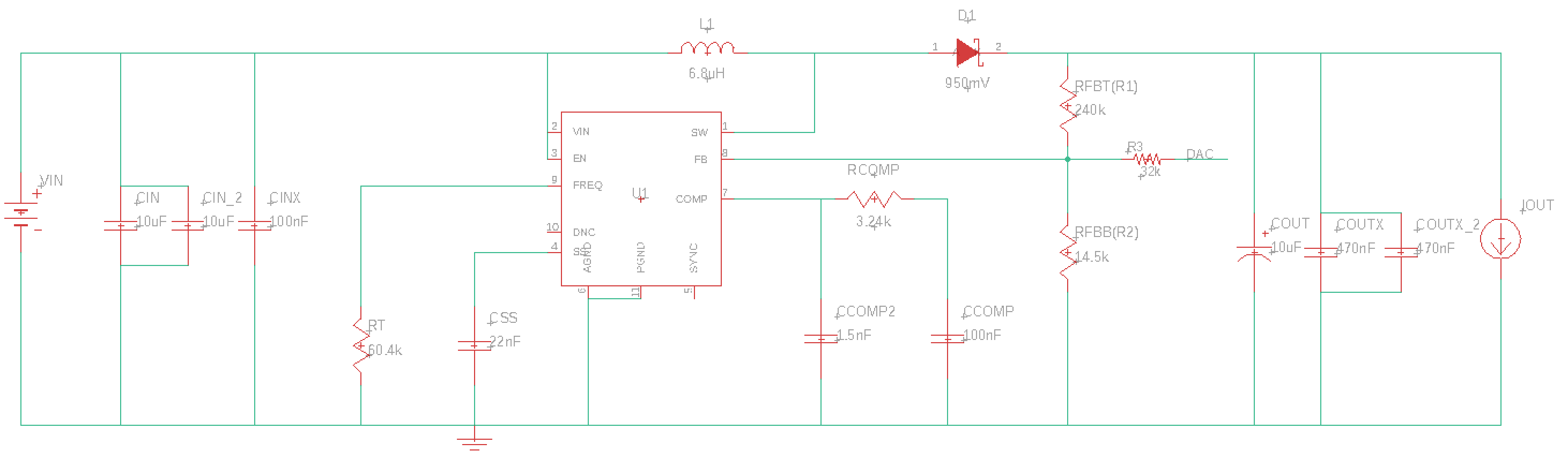
I followed the WEBENCH's schematic and PCB layout for my prototype.

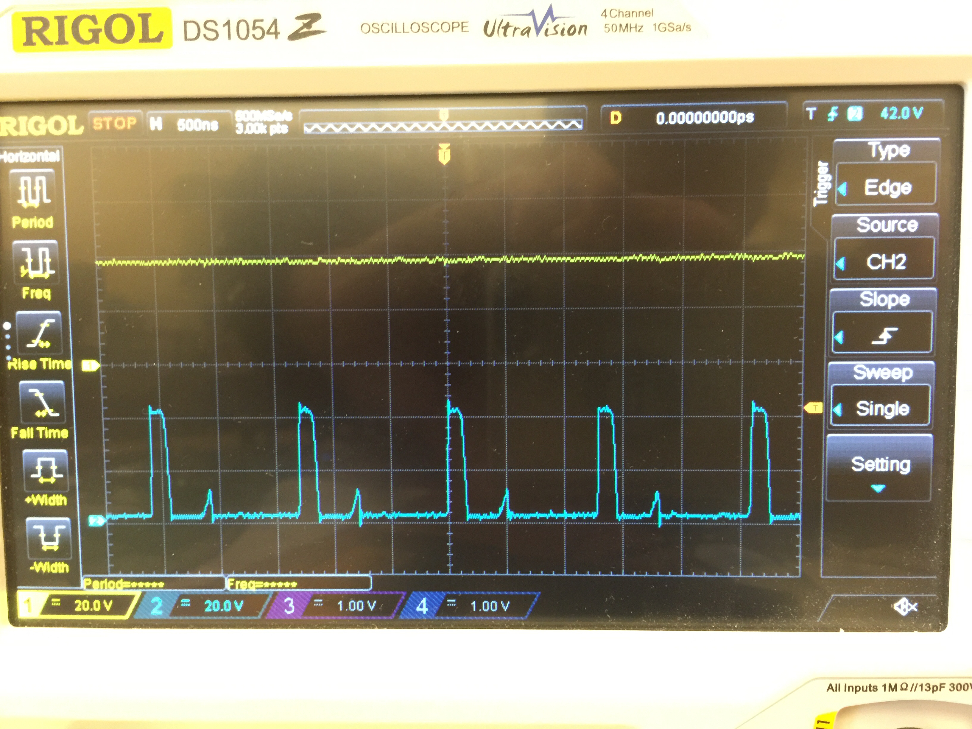
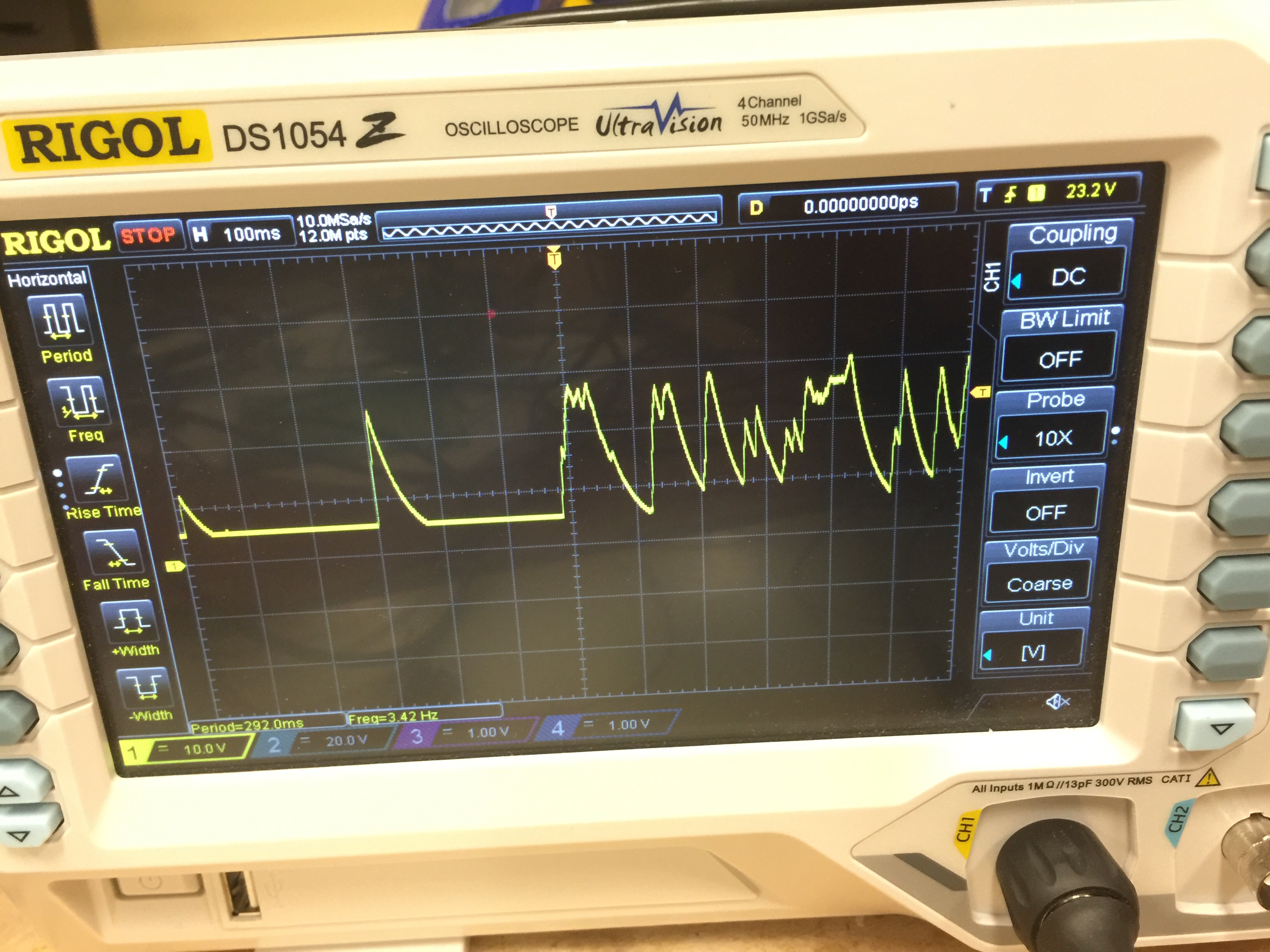
I was expecting to get 30.6V output when I plug the USB 5V input. However, I get an output way lower than 30V.

When the "DAC labeled" part is 0V (connected to GND), the output is

0. VIN = USB 5.06V, EN pin = USB 5.06V, VOUT =  9.24V

1. VIN = USB 5.06V, EN pin = 3.288V, VOUT =  4.89V

May I ask

Q0. Why am I getting these output instead of 30.6V? Hope is not a layout issue.

Q1. I wanted to toggle the EN pin using a 3.3V microcontroller.

However, when I connect 3.288V to the EN pin, the output becomes lower than the input voltage.

Does the EN pin has to have the same voltage as the VIN input voltage?

Funny thing is even EN pin is equal to VIN, the output shows an unexpected value.

  • Hi David,

    Q0: Please share the layout to check.

    Q1 EN threshold voltage(maximum) is 1.30V so the 3.3V microcontroller should be easy to drive EN pin to logic high. 

    When DAC is 0V, the lower feedback resistance is 14.5k paralleled with 32kohm, so it is 9.97kohm. The Vout should be (240/9.97+1)*1.129=28.3V.

    Can you check the FB pin, SW pin, Vout waveform?

  • Hi, Zach. I wish to make some updates.

    This is the current schematic I use. I use TPS55340PWPR.

    The WEBENCH recommended me to use B560C-13-F 60V Schottky diode and the 4.7uH XAL5030-472MEB inductor.

    All the resistors have 0.1% tolerance with 1/8W Power rating and 0603 (16mm x 08mm) size.

    The Switching Frequency is 0.779MHz. Pin 6 SYNC and 7 AGND are connected to GND, which is also connected to the PAD and the PGDN (Pin 11, 12, 13, 14).

    Top PCB (purple comment shows the plain like GND plain)

    Bottom. This is a 2 layered PCB.

    After I resoldered the boost converter, it did show 38V from the output.

    Probe 1 Yellow: VOUT 38V, Probe 2 Blue: SW pin (FB is1.129V).

    Currently, I only added two 10uF Aluminum Electrolytic Capacitors at VOUT.

    However, this didn't last long. After like 20 seconds, VOUT fluctuates.

    I thought this was a temperature issue since I didn't add thermal vias. However, the boost converter was 34°C (93.2 °F) max.

    Sometimes I hear "beep" sounds from the board; I think it is coming from the Schottky diode.

    So this does work for a few seconds. What seems to be the problem?

  • Hi David,

    The schematic looks good but layout is bad. 

    1. The traces between polygon and IC pad is too thin so it cannot handle large current and it's bad for power dissipation. 

    2. Place Cin close to IC and power inductor. One 1uF ceramic output capacitor is recommended for better output voltage ripple. Please refer to datasheet part 10 for detailed layout instructions. 

    Have you checked the IC temperature with thermal imager?

  • Thanks, Zack

    Zack Liu said:
    Have you checked the IC temperature with thermal imager?

    One moment; I'm trying to borrow one. At least the Infrared thermometer

    is telling me the boost converter was 34°C (93.2 °F) max. The datasheet said "Wide –40°C to 150°C Operating TJ Range".

    Zack Liu said:
    1. The traces between polygon and IC pad is too thin so it cannot handle large current and it's bad for power dissipation. 

    Thanks for the feedback. I'll change the trace.

    Zack Liu said:
    2. Place Cin close to IC and power inductor. One 1uF ceramic output capacitor is recommended for better output voltage ripple. Please refer to datasheet part 10 for detailed layout instructions. 

    Hmm, I'm using the TPS55340PWPR (14-Pin HTSSOP PWP Package). Seems like the datasheet only describes the layout for RTE Package, 16-Pin WQFN.

    For the EVM case, the CIN should be C7 and C7 is right next to the boost converter.

    Q1. In my case, C2 is the CIN. The distance between C2 and pin 3 VIN is 3.13mm. Do you mean I have to move this closer?

    I wish to know what is the acceptable distance to think it is close enough.

    Q2. "Minimize the length and area of all traces connected to the SW pin and always use a ground plane under the switching regulator to minimize inter-plane coupling."

    Does this mean the SW plane has to be smaller? I'm curious whether I have to decrease the SW plane on my PCB.

    Also, below the SW plane, do I have to place the GND plane right below from the SW plane?

    Since I'm using a 2-layered PCB, can I ask a guide for the bottom layer?

    Q3. "To prevent radiation of high-frequency resonance problems, use proper layout of the high-frequency switching path."

    I cannot find descriptions related to this high-frequency switching path; what type of "high-frequency switching path" layout is required?

    Q4. From the EVM, "Nine vias directly under the TPS55340 device provide a thermal path from the top-side ground plane to the bottom-side ground plane."

    Can I ask the guideline for the thermal vias on the pad; how many vias and what hold size is recommended?

    Q5. All the feedback resistors for creating VOUT have 0.1% tolerance with 1/8W Power rating and 0603 (16mm x 08mm) size. Is the power rating sufficient enough?

    Q6. Currently, I only added two 10uF Aluminum Electrolytic Capacitors at VOUT.

    May I ask why a ceramic output capacitor is recommended for better output voltage ripple?

    Q7. When I apply GND 0V to the EN (enable) pin, I observed VOUT becomes equal to VIN.

    I was hoping the boost converter to provide 0V output when disabled.

    Is this an expected behavior? If so, is there a way to make the output to be 0V?

  • Hi David,

    Please see my comments below:

    Q1: Place 0.1uF C2 close to IC for decoupling. Now C2 place is good. No need to change it. Place CIN(10uF+10uF) and COUT( 470nF+470nF+10uF) like below picture.

    Q2: The SW plane of your board is a little bit big, but won't affect the normal switching. Only need to widen the trace. In altium designer, you can change the polygon connect rule to direct.

    Q3: The high frequency switching path is VIN->inductor->SWpin->GND->Cin, and VIN->inductor->diode->Cout. So that's why I ask you to put CIN, COUT closer.

    Q4: Hole size 10mil. Diameter 20mil. 9 vias is enough.

    Q5: 0603 size is big enough.

    Q6: Yes. Ceramic has less ESR, ESL than aluminum capacitor.

    Q7: When EN pin is 0V, current will go through Vin, inductor, diode, Cout. So Vout will euqal Vin. If you need true disconnection feature, you may need to use another boost converter device. Can you let me know your application's Vin range, Vout, Io and other requirement?

  • Thanks, Zach.

    Zack Liu said:
    Only need to widen the trace. In altium designer, you can change the polygon connect rule to direct.

    I'm using EAGLE 9.

    For comparison, I removed the "thermal relief" (polygon trace) to swallow the GND pads.

    I left other traces as the same intentionally to ask you these questions.

    Q1. As you see the GND pads, can I remove the thermal relief like the above picture?

    Or is it mandatory to have a thermal relief? If so, I wish to know what width do you recommend for widening it.

    Zack Liu said:
    Place CIN(10uF+10uF) and COUT( 470nF+470nF+10uF)

    Q2. Can I populate a single Ceramic CIN 22uF cap and Ceramic COUT 22uF?

    Are you considering the ESR & ESL as well for these shunt (parallel)  capacitors?

    Zack Liu said:
    Q4: Hole size 10mil. Diameter 20mil. 9 vias is enough.

    Q3. My board house can handle

    Hole size 0.3mm (11.811mil), diameter 0.6mm (23.622 mil) minimum.

    Every thermal vias' size is following the minimum specification and P$5 is centered to 0, 0 (X, Y)

    P$1: -0.9mm, 0.8mm / P$2: 0mm, 0.8mm / P$3: -0.9mm, 0.8mm

    P$7: -0.9mm, -0.8mm / P$8: 0mm, -0.8mm / P$9: -0.9mm, -0.8mm

    Is this an acceptable arrangement?

    Q4. Do I need to apply solder mask to the thermal vias?

    Also, is it required to create thermal pad on the bottom layer?

    Zack Liu said:
    If you need true disconnection feature, you may need to use another boost converter device. Can you let me know your application's Vin range, Vout, Io and other requirement?

    - VIN: 2.9 ~ 5V (I want to use either 3.3V like voltage source / Li-ion battery / USB 5V)

    - VOUT 30 ~ 38 V (38V is the best, I'm going to use the PMP15037/DAC signal to decrease VOUT)

    - Io 120 ~ 240mA, 240mA will be the best

    - Any switching frequency is acceptable

    - Footprint size doesn't matter, less than 25mm x 25mm is preferrable

    - Don't want ball grid type of packages

    - Considering 2 layered PCB

    - Wish an ENABLE pin that can create 0V if possible

  • Hi David,

    Please see my comments below:

    Q1: Please remove the thermal relief.

    Q2: Single ceramic is enough. Ceramic capacitor has lower ESR so input & output voltage ripple will be smaller.

    Q3: Place thermal vias under IC thermal pad and close to PGND pins. Heat would be passed to bottom layer through vias. 

    Q4: You don't need solder mask for thermal vias. Put a GND polygon on bottom layer like you did in the first layout.

    I go through all existed boost converter products but cannot find another device with true disconnection feature. You can add a load switch after TPS55340.

  • Thanks, Zach. Before closing this, I wish to double-check.

    Zack Liu said:
    Please remove the thermal relief.

    Like this picture, right; swallow the GND pads inside the plain? For other plains (SW, VIN) as well?

    Zack Liu said:
    You can add a load switch after TPS55340.

    Something like this? Since I want a 38V output from the boost converter with a 3.7V Li-ion battery,

    can you recommend one of TI's load switch, please? The price/package/footprint size doesn't matter.

  • Hi David,

    Yes. For all power pins, like GND, SW, VIN, please connect polygon to pins directly without thermal relief. 

    Before the next PCB manufacture, you can share the layout here and let me check it.

    I would like to give you a suggestion but I'm only supporting boost converter products. You can post a new thread on E2E forum and the load switch applications engineer will give you a good answer. Thanks.