This thread has been locked.

If you have a related question, please click the "Ask a related question" button in the top right corner. The newly created question will be automatically linked to this question.

LM73606: Potential reasons for light load power-to-ground short failure.

Part Number: LM73606

Hi support,

I recently had an LM73606 destructively fail with a power-to-ground short. I do not see any immediately obvious reasons for this to happen and would like ideas of where to look.

The type of answer which would help me most is a list of causes which may cause the chip to fail in the way described below; including:

  • anything that might happen from a hand placement and soldering job, assuming the proper tooling
  • input power supply transients
  • output power transients

Circuit Description

The LM73606 is configured in a ground-referenced buck topology to produce a non-isolated -7V power net. it is used in conjunction with an additional LM73606 to produce a similar +7V power net. Both chips are being powered by the same +24V power supply, which produces a 31V supply for the -7V regulator.

Though I can not attach these portions of the schematic publicly, the converters are being used to power a small number of ADCs and DACs, one linear DC-DC converter each, and a pair of power amplifiers. The power amplifiers are the main current draws in the circuit; the way they are being used should only place a significant draw on one converter at a time. The total current for these operations are well within the LM73606's ratings.

Failure conditions

At the time of failure, the failed converter had been powered for roughly 20 minutes and had been operating normally. The output of the power amplifier had been commanded for +20mA, which is to say the failed converter should have been essentially idling.

Now that the converter is failed, there is:

  • a 6ohm short from PVin to PGND (nets named SupplyB_P to -7V)
  • no short from PVin to the SW node
  • no short from SW node to to PGnd
  • no additional shorts in the LM73606 to either PVin to PGnd
  • no shorts anywhere else in the circuit.

The only potential defect I can see is that there might be poor solder contact on the sync/mode pin.

This one is kind of a head scratcher for me.

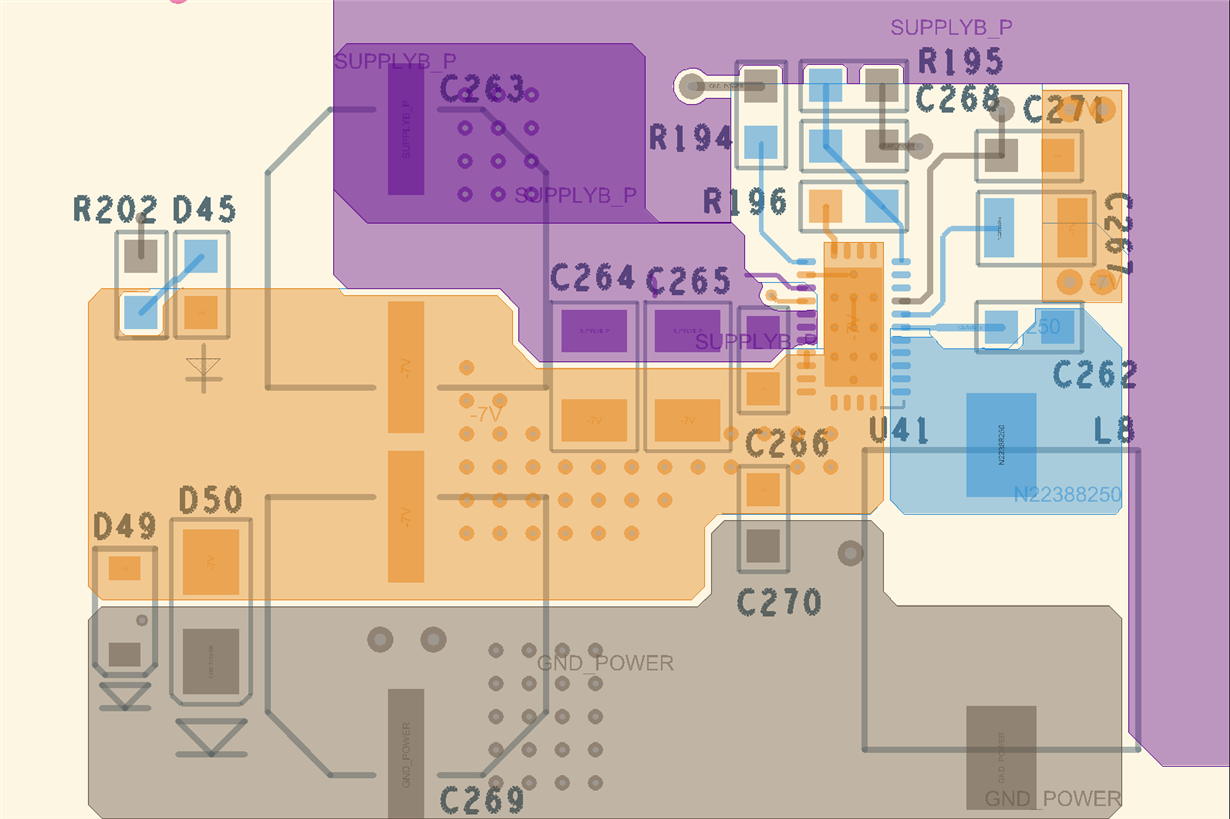
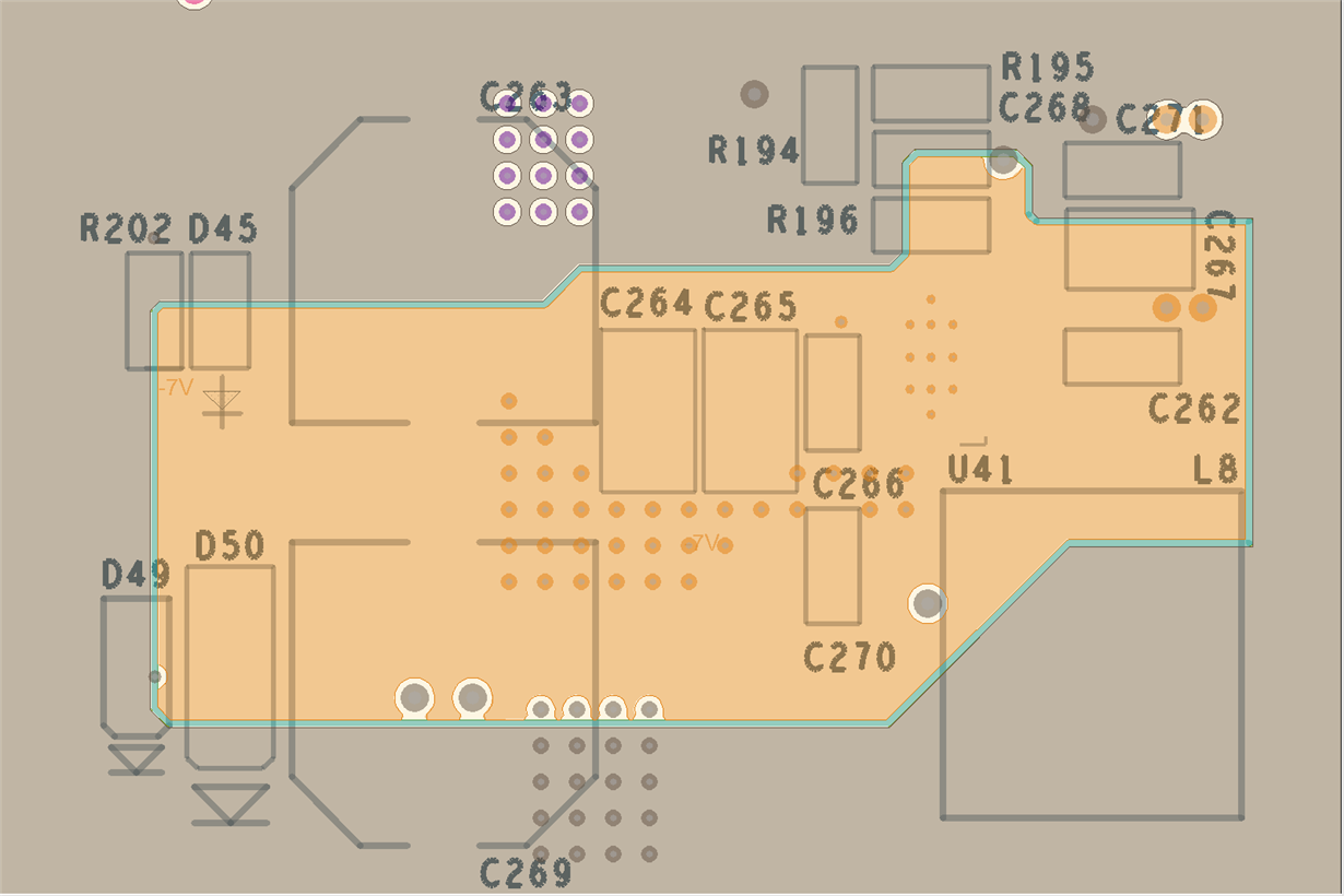
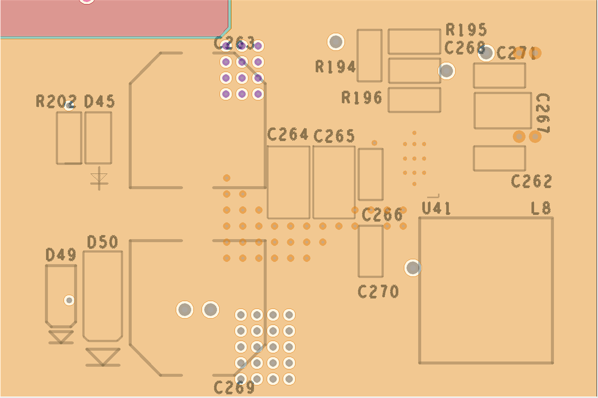
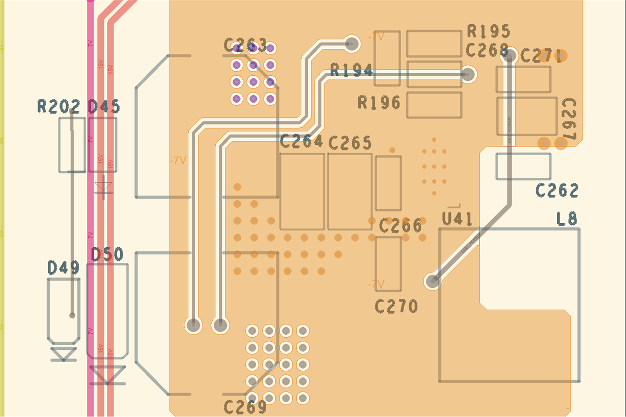
I've attached portions of my schematic detailing the power inlet and the converter itself, images of my layout, and photographs of the failed chip.

Power inlet

LM73606 converter circuit

Layout - Top

Layout - Gnd

Layout - Pow

Layout - Bot

  • Peter,

    The schematic looks good. The layout looks good.

    You listed the main possible causes but here's my list:

    • Voltage exceeding abs max in datasheet on a pin. Your 24V to -7V should have enough margin but please check the switch node and VIN for ringing that may exceed the abs max voltage.
    • ESD
    • Accidental shorts due to soldering or assembly - Your picture shows some shiny debris between pins 19 (AGND) and 20 (PVIN). This is probably from the issue event but it may have caused the event if it was there before.

    We have not seen an issue like this on this part. We are not able to come to a definitive conclusion based on the information provided. Please continue evaluation with those bullets in mind.

    -Sam

  • Hi Sam,

    Thanks for taking my question. I appreciate your response.

    We'll undertake an investigation in to the switching node voltages.

    Just to follow up with those suggestions, though, I'd like to recall your attention to the fact that the kOhm impedances are intact between the switch node and both PVin and PGnd nodes. More than that, the damage to the package is not physically located near the switch node pads.

    Therefore, my main question is: what can fail in the IC between PVin and PGnd pins?

    Perhaps I can use this information to help backtrack the reason it failed.

  • Peter,

    It's possible that a SW abs max violation can cause this. There is other circuitry on SW which may become damaged which can cause a soft short from PVIN to PGND with no apparent short from SW to these pins.

    Have you compared the resistances of this IC to a known good IC? That will tell you with more confidence if the values you're reading are normal.

    You may also check, as you mentioned, the connection from SYNC/MODE to the board. The datasheet states not to float this pin. If it was floated due to poor soldering, the part may keep switching between modes and could cause issues but I doubt that would cause a blow-up.

    -Sam

  • Peter,

    How is the testing going?

    -Sam

  • Hi Sam,

    I've checked the good converter's FET impedances, these impedances are nearly the same value as the blown-converters FETs.

    Also checked the switch node, in normal operation, I've got a Vpk-pk voltage of 34V. I did not capture a scope trace of the start up behavior, and I don't have a captured scope trace on hand. I'll try to get back to the lab soon to observe the start up behavior.

    As far as shape, the switch node voltage is almost a dead-ringer for Fig 59 in the datasheet, except with the peak voltage above.

    Regarding the sync/mode pin, I don't have a good way of testing the connection. The pin flank is too small for the probes we have in house.

    I need to take a second look at the switch node, I'm a little surprised to see it as high as 34v, I'd have expected 31v.

    If you have any additional suggestions, I'll be happy to hear them.

    Thanks again.

    -Pete

  • Pete,

    I agree, take a second look at the switch node. Maybe the +24V supply overshot which could cause SW to exceed its rating. Keep me posted on progress.

    Note: Threads lock after 30 days from the initial post. If this continues past the 30 day mark, please post a new thread and refer back to this one. Thanks.

    -Sam

  • Hi Sam,

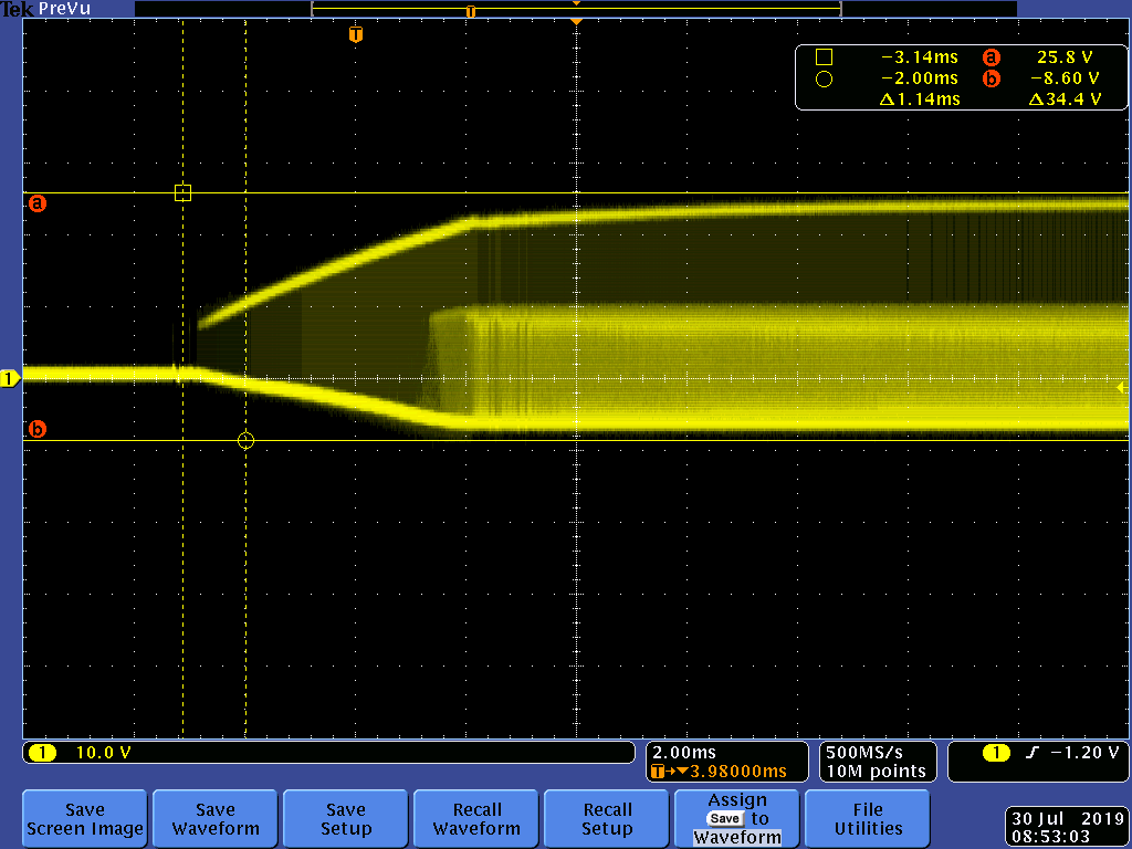
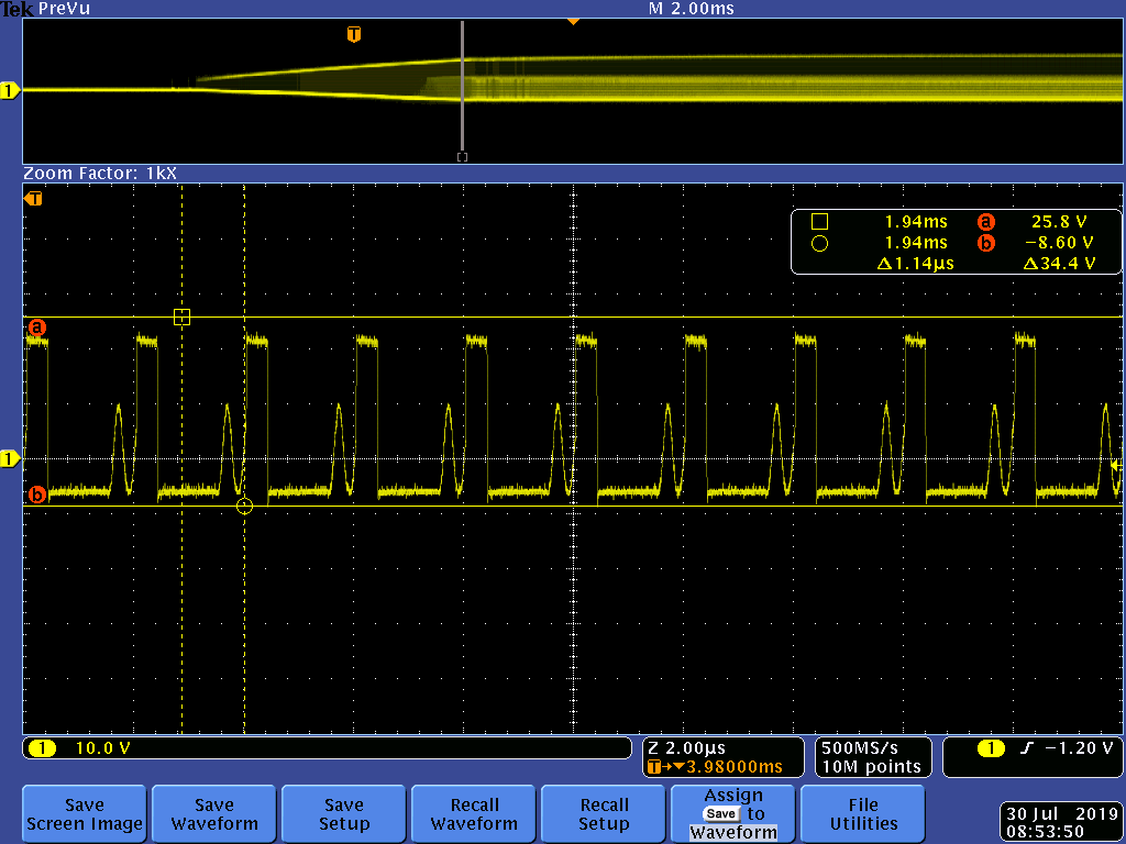
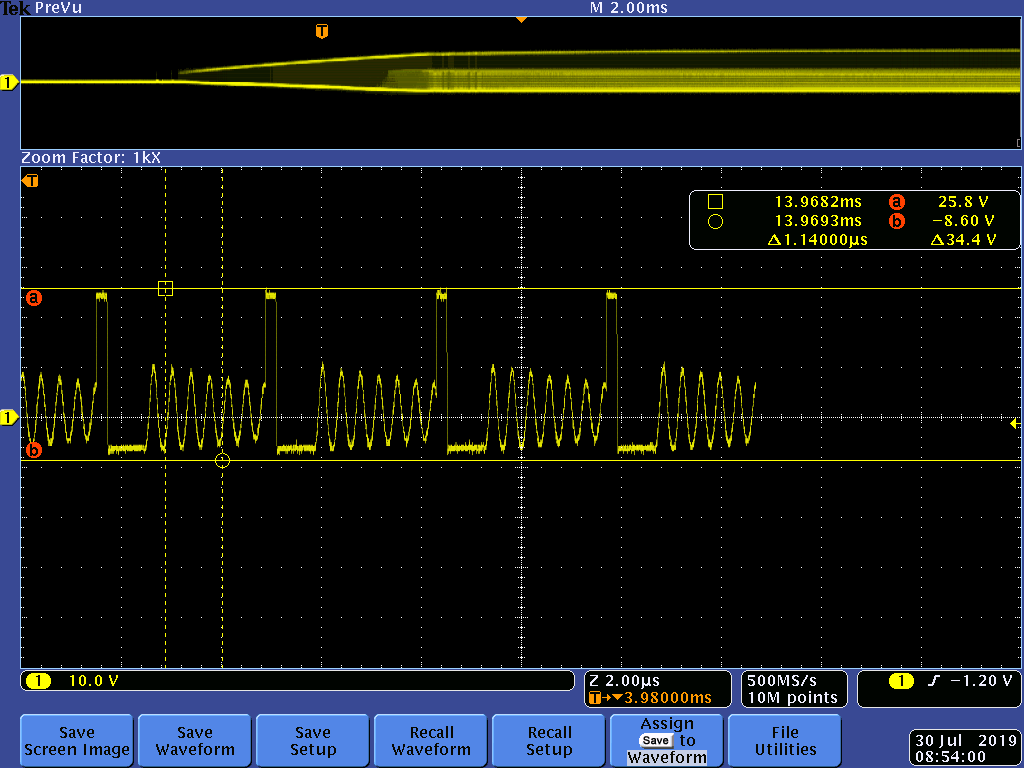
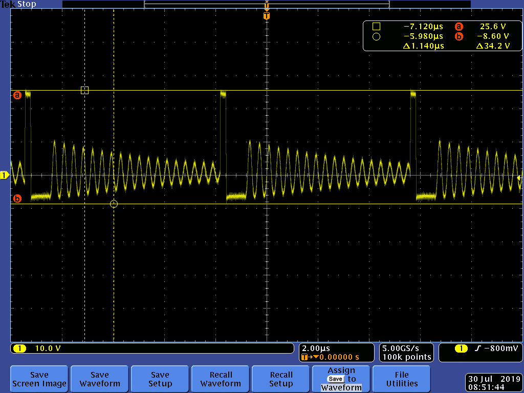
    Had some time to get in to the lab this AM and grabbed some scope shots. All of what follows are taken from the lead of the SW node of the inductor.Probe Point Illustration

    Start up of the converter:

    Detail #1:

    End of start up trace:


    Steady State:

    Looking at these scope traces, I did not see anything completely awful, I'm a little concerned that the Vpk-pk is as high as it is, but it is still within the limits of the converter. The counter argument to that is this is a a totally different board where the converter has not failed.

    Thoughts?

  • Peter,

    The waveforms look good. It may be useful to zoom in to a single rise and fall of the SW node. That way we can see any overshoot with more detail.

    But if the voltage across the converter is 34V, the converter should be fine.

    Make sure you are using the tip-and-barrel method or a differential probe with very short wires to keep the waveform as true as possible.

    It may be time to investigate possible ESD, handling issues, soldering issues, or other ideas. 

    -Sam