This thread has been locked.

If you have a related question, please click the "Ask a related question" button in the top right corner. The newly created question will be automatically linked to this question.

TPS546C20A: power up

Part Number: TPS546C20A

Hi,

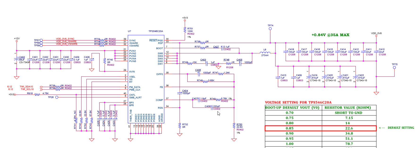
I'm trying to power up the device but i went through the datasheet so look likes i need to program the part before i can power up. Am i correct?

Please help to confirm this.

Thanks

  • Tuan,

    The TPS546C20A should power up to the default states of the registers.  Are you using the TI EVM or your own design?

  • Hi John,

    It is my own design. Is it support to power up to default states without programming it? Am is correct ?

    Thanks,

    - Tuan D. 

  • Tuan,

    Yes it should power up in the default state.  Make sure you do not have any external connections that would contradict them such as VOUT_SCALE_LOOP is default to "1", which requires no external resistor divider network.

  • Hi John,

    I don't have Rbias on our design but i can't see the V_out. Is there any recommendation for this?

    Thanks,

    - Tuan D.    

  • Hi John,

    I also have one more question. I don't GUI support for this device on Fusion Design software. Please provide where i can download this

    Thanks,

    - Tuan D. 

  • Tuan,

    I have someone looking into this.  we'll get back to you as soon as we can.

  • Tuan,

    Are you trying to start a new project file for the TPS46C20A, or are you connecting the TPS546C20AEVM to a computer with the USB2GPIO dongle and the FUSION GUI is not discovering the TPS546C20A through its automatic scan?

  • Hi Peter,

    I'm using USB interface Adapter connects to the laptop but The Fusion GUI doesn't recognize my adapter. Is there any recommendation?

    Below are software and adapter that i use:

    1- https://octopart.com/usb-to-gpio-texas+instruments-2449062

    2- http://www.ti.com/tool/FUSION_DIGITAL_POWER_DESIGNER.

    Thanks,

    - Tuan D. 

  • Tuan Dang,

    You said the GUI is not recognizing your adapter?  Are you getting an error message when you launch the On-line FUSION GUI? 

    If so, what is the error message you are receiving?

    If not, please describe the sequence of steps you are following, and what you are seeing so we can help debug it for you.

    Is the Adapter plugged into a USB port?

    Is the green LED on the end of the Adaptor "on" ?

    If you order the Adapter from TI.com or from Octo-parts?

  • Hi Peter,

    I got this message. Please see the attached

    I also see the green LED on

    Yes we got it from distributors

    Thanks,

    - Tuan D. 

  • Tuan D,

    This indicates that FUISION is seeing the dongle and it is working, but that it is not detecting a compatible device over PMBus.

    FUSION uses a scanning technique where it repeatedly reads a PMBus command from each PMBus address, looking for a recognized response to identify the part.  The TPS546C20A uses IC_DEVICE_ID to identify the part.  In the FUSION GUI "Device Scanning Options" you  should have an option to scan IC_DEVICE_ID.

    Try  "Change Device Scanning Options" and selecting IC_DEVICE_ID for the scanning option.

  • Hi John,

    I'm trying but i still got same problem. Please see thea attached and recommendation. 

    Which one should i select?

    Thanks 

  • Tuan,

    Try setting the first (1d) box to 4620h and then try.

  • Tuan,

    Is the TPS546C20A EVM powered up?

    The TPS546C20A requires AVIN, which is powered from the Evaluation Module's primary input voltage - VIN, to be powered in order to enable PMBus Communication.  It can not power up from the 3.3V output of the USB-to-GPIO dongle, so it needs a separate 4.5V-16V power supply to power the IC and enable PMBus communication before the dongle will detect it.

  • HI Peter/John,

    I'm not sure it is powered up. 

    I have 12V input PVIN and CNTL 3.3V always pull up. 

    I'm trying to get 0.8V from the output. I can not get it. I don't understand why?

    Does this chip need to program to get V_out? That's why I'm trying to program it.

     Is there any recommendations to fix this issue? 

    Thanks,

    - Tuan D.  

  • Hi Peter/John,

    Please see attached image for V_out 0.8V. It looks keeping reset. So how to get RESET to stable?

    Thanks,

    - Tuan D. 

  • The waveform shows the output voltage only getting up to about 300mV with each reset attempt.  That would generally indicate an over-current condition.  The ~ 20ms reset timing is also correct for an over-current condition, but the output voltage is discharging at about a 10ms time constant, which would not be indicative of an over-current unless the 300mV is below the compliance voltage of an external load.

    Is there a load connected to the board?

    What is it set to?

    Have you used an oscilloscope on the input to make sure the input voltage is not collapsing when it tries to charge the output capacitors?

  • I should have also asked, have you gotten he part to talk to the FUSION GUI now?

    If so, what is the Fusion GUI reporting as faults coming from the IC?

  • I'm using the part as the default setting so I don't program this part.

    Please see the input waveform. It seems 12V input is not stable, it may cause the output.

    Please advise. 


  • Tuan Dang1,

    Your e-mail about the output voltage was taken at 20ms / division and shows a period of just over 1 division, this shows 1ms/division, also with a timing of 1 division, that would not be consistent with the input voltage ripple being caused by the output voltage ripple.

    Is this one of the EVMs?  If so, which one?

    If this is not one of the EVMs, do you have the circuit that it's using?

    Is anything connected to the output?  If so, what?

  • HI Peter, 

    Please see the attached schematic. 

    Please advise

    Thanks,,

    - Tuan D.  

  • Tuan,

    I have alerted Peter to have a look.

  • Tuan,

    In the mean time try removing R750.  Let me know if this works.

  • Hi John, 

    I removed R750 but it didn't work. 

    Thanks,

    - Tuan D. 

  • Tuan,

    Where did the compensation values between DIFFO, FB, COMP and AGND come from?  They don't appear to be stable give the output filter you have.

    Try updating the following component values:

    1) Remove R750 (FB to AGND resistor)

    2) Change R748 (DIFFO to FB) from 3.65k to 10k Ohms

    3) Change R747 from 1.24k to 442 Ohms

    4) Change R749 from 5.76k to 3.32k Ohms

    6) Change C406 from 1000pF to 4700pF

    7) Change C407 from 1.8pF to 8200pF

    8) change C408 from 220pF to 390pF

    Based on the listed output filter and about 10mOhm per 470uF electroluytic capacitors, that should give you a bandwidth of about 40kHz with sufficient gain and phase margin for stable start-up and operation.

    Also, have you managed to get the part on the board talking to the FUSION GUI through the PMBus dongle?

  • Hi Peter,

    Thanks for your feedbacks

    Based on the datasheet, if you set it as default sate, you don't need to program it so that's why i don't use the part on the board talking to the FUSION GUI through the PMBus dongle. Am i correct?

    Let me try to remove and change based on your suggestion and let you know if it works.

    Thanks,

    - Tuan D. 

  • Tuan,

    While you don't need to program the TPS546C20A device prior to powering it up, communicating with the device via PMBus can provide valuable indications about programs, such as flagging the cause of faults using the status bits, reporting telemetry, etc.  I wanted to know if you were able to get the TPS546C20A to communicate with the FUSION GUI or not.

  • Peter,

    I was trying to get the TPS546C20A to communicate with the FUSION GUI but it didn't work.

    Thanks,

    - Tuan D. 

  • Hi Peter,

    I have updated components values, and I got 0.8V Vout but the ripple too much. 

    Please see attached and recommend to reduce this. 

    Thanks,

    - Tuan D. 

  • Tuan,

    The ripple is, indeed, unusually high.  The first couple of "jumps" appear to show about 250-270mV of amplitude.  The schematic shows 646uF of ceramic capacitance for 161.5uC of charge (I am not including the 4x 470uF capacitors here as their ESR might be high enough to minimize their charge absorption).  That represents a full 350kHz on-time for 12V input 0V output.  Unless those 470uF capacitors have very high ESR, something is significantly wrong in the circuit.

    1) Check the layout. 

    Are all of the output capacitors shown in the schematic close to the converter's inductor?

    Do they all have good connections to ground?

    Is the oscilloscope's ground connected to more than 1 point?

    Is the board ground connected to "Earth" ground at more than 1 point?  (Keep in mind Oscilloscopes connect their ground input from all 4-channels together inside the scope and to the center "Earth Ground" pin of their outlet.  If the power-supply powering the board is also connected to "Earth" ground it will create multiple ground connections on the board.

    2) Check the connections

    Check the soldering of the output capacitors to make sure they are all soldered to the board well

    Is the remote sense point where R736 connects to VDD_0V8 close to the inductor?  Far away from the inductor?

    Is the remote ground sense point where R732 connects to ground close to the output capacitors?  Close to the inductor?  Close to the TPS546C20A IC?

    3) Check the components

    Using an oscilloscope setting of 2us / division, measure SW and VOUT on the same image with 2V / division for SW and 50mV/division for VOUT.

    Set the VOUT channel to DC coupling and adjust for an 800mV offset so that the output ripple is clearly visible.

    I am looking for the shape of the output ripple with respect to the switching waveform.  The output ripple will be made up of 3 components:

    A Square Wave representing the output capacitors inductance (ESL)

    A Triangle Wave representing the output capacitors resistance (ESR)

    A Sine Wave representing the output capacitors capacitance (Cout)

    I am also looking for the stability of the pulse width from one switching cycle to the next.

    4) Do you have access to a network analyzer or bode-plot sweep tool that we can use to measure the power-stage loop performance if we decrease the bandwidth of the compensation to stabilize it, so we can see what the L-C filter with PCB parasitics looks like?

    5) Are you able to share your PCB layout?

  • Tuan,

    This thread has been inactive for a while.  I will go ahead and close it.  You can re-open at any time.

  • Thanks John, 

    I will work on this. I will let you know if I have any questions. 

    Thanks again for all your help.

    - Tuan D.