Hi team,
I'm checking about Input channel selection and ST pin with TPS2121EVM-023.
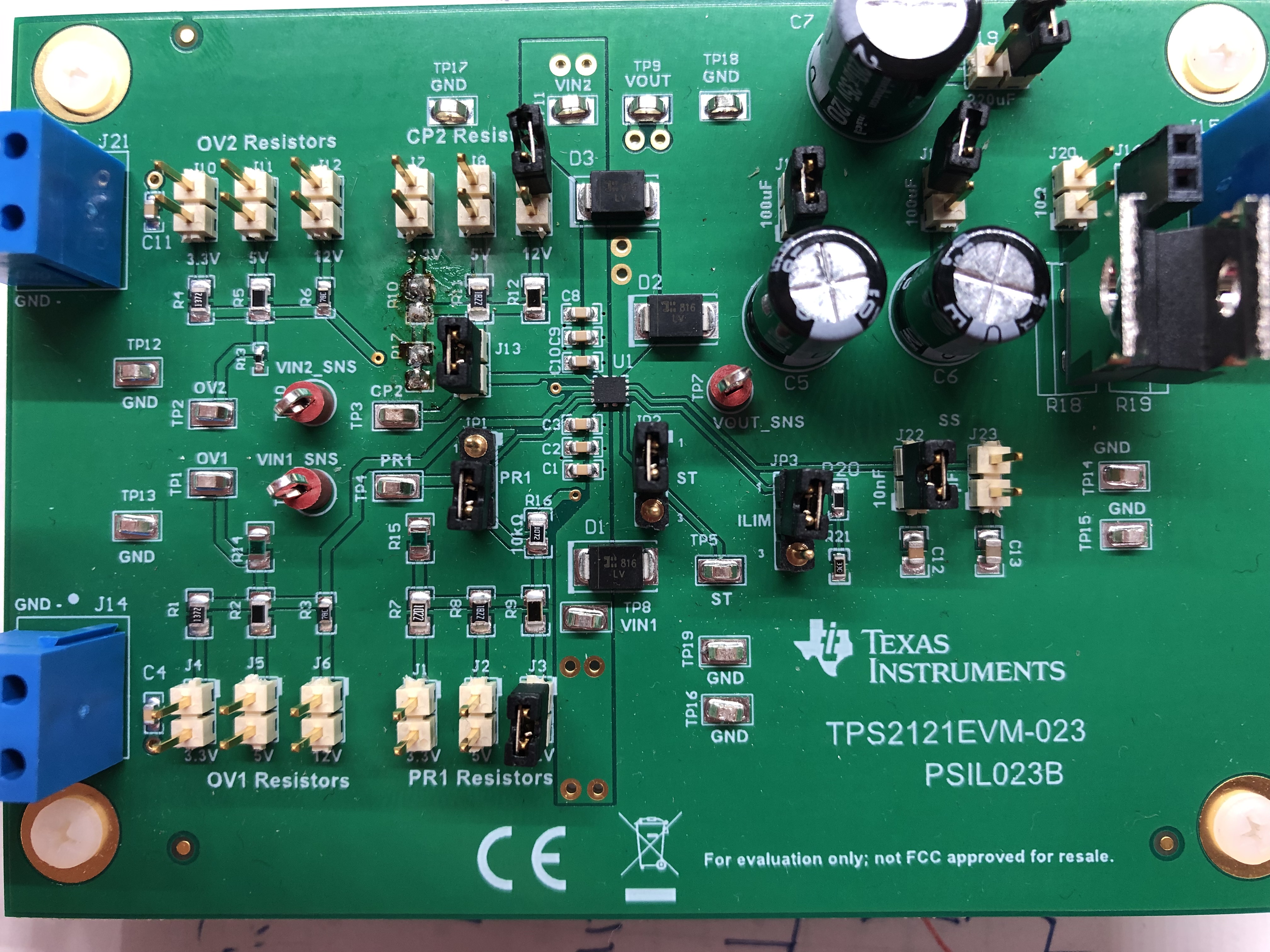
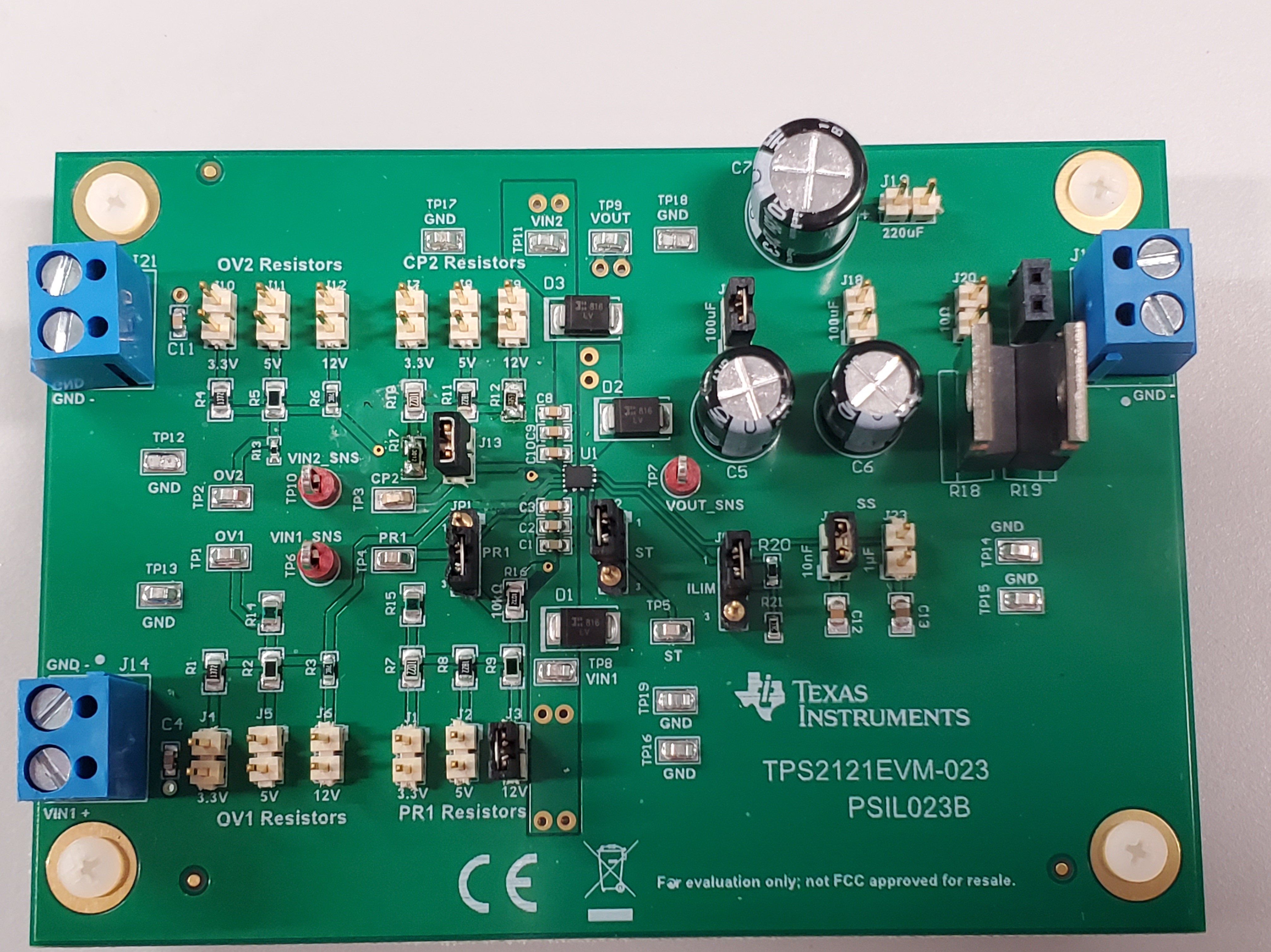
Fig.1 is my circuit and Fig.2 is my environment.
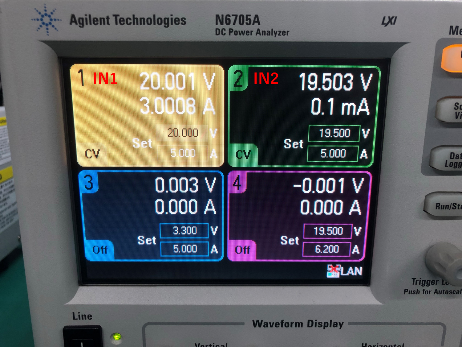
I operated that IN2 was valid after IN1 was valid.
I guessed the IN2 was selected and ST was low because CP2 was higher than PR1.
Datasheet (excerpt):
>If PR1 > CP2 then IN1 is used, and if PR1 < CP2 then IN2 is used.
>ST is pulled high when the output is Hi-Z or IN1. It is pulled low when IN2 is powering the output.
However, according to Fig.3 and Fig.4, IN1 still loaded current (3A) even though ST pin was low.
How come this situation occurred?
Fig.1 Circuit :
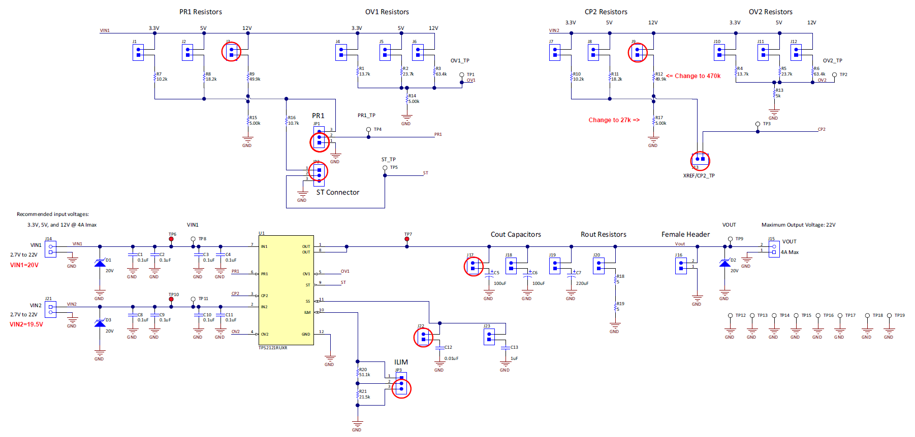
Fig.2 Environment:
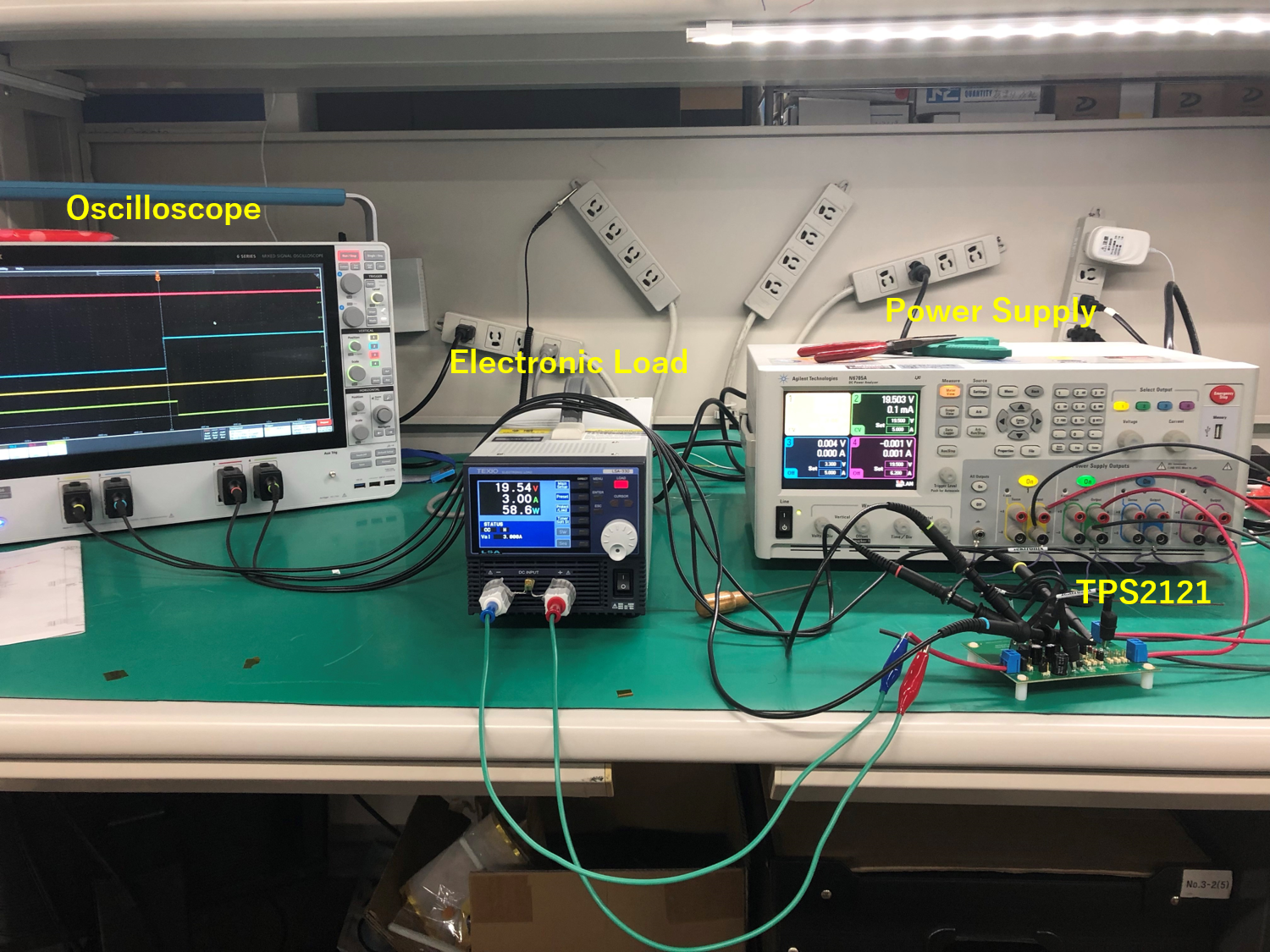
Fig.3: Oscilloscope
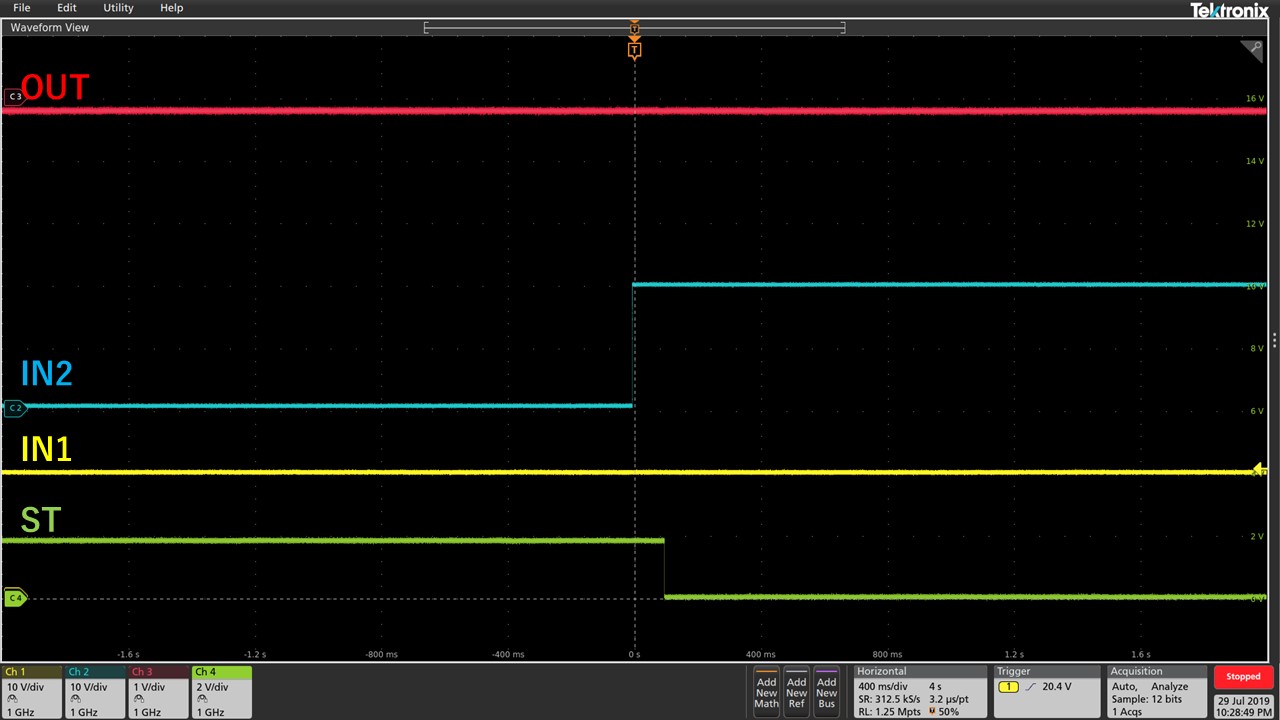
Fig.4: Electronic Load