This thread has been locked.

If you have a related question, please click the "Ask a related question" button in the top right corner. The newly created question will be automatically linked to this question.

TPS546C20A: Two Phase Buck converter debug problem

Part Number: TPS546C20A

Hi:

I am using TPS546C20A to design a two phase stackable synchronous buck converter.the input is 12V,output is 5V/70A.

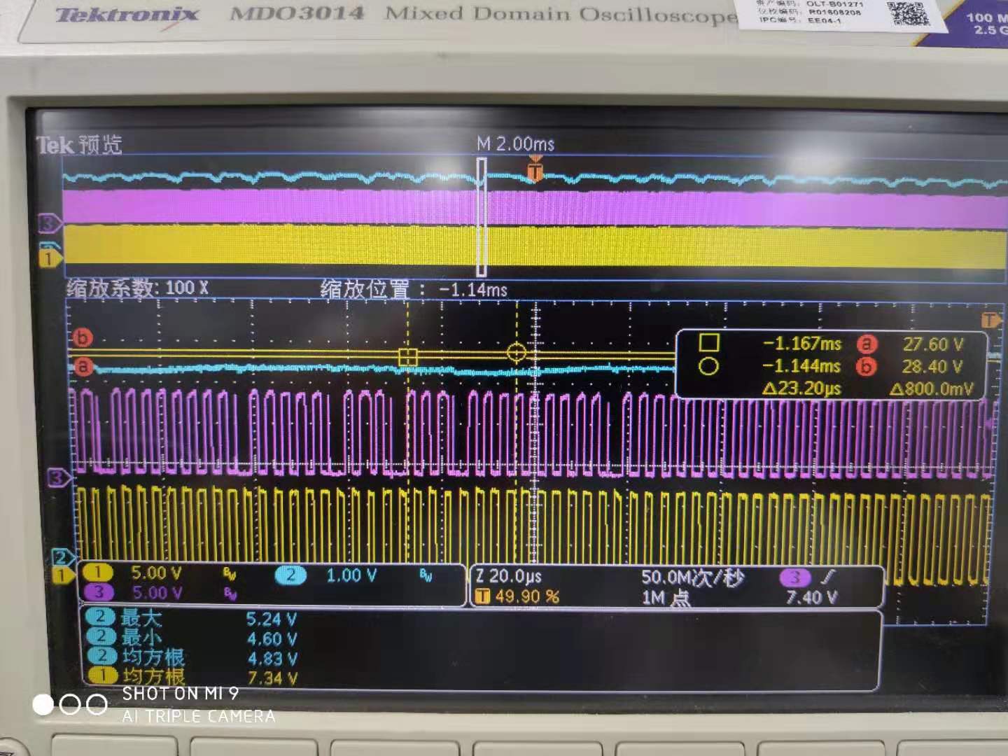
when I increase output current up to 45A,the slave SW voltage will  decrease pulse  width periodically,but master SW voltage is OK.and more current will shutdown the converter.+5V output voltage can't stay stability;

CH1:master SW         CH2:+5V          Ch3:slave SW

  • User,

    We will look into this.  Can you share your PCB layout?  Also, this looks like a duplicate post from another user, Mark Xing.  Do you know about it?

  • User,

    The TPS546C20A has a high-side Over Current Protection circuit that monitors the voltage drop from AVIN to SW during the switch-node on-time and terminates the switching pulse on SW for the remainder of the switching period if it detects excessive drop from AVIN to SW.

    Check the voltage on AVIN of the slave device, particularly the ripple on AVIN compared with the timing of the SW node and the PVIN node.  It is likely that AVIN at the IC pin is not dropping as much as PVIN is dropping at the IC pin, and that the slave device is triggering a high-side OC protection, terminating the PWM pulse early and causing the output voltage to drop.

    if that is the case, you may need to either adjust your layout so that AVIN and PVIN track closer together during switching, or add a resistor from PVIN to AVIN, sized large enough to create a drop from PVIN to AVIN that is equal to or greater than the ripple on PVIN.

    It should also be noted that, in addition to the main 22uF capacitors from PVIN to PGND, it is recommended that designs include a 2.2-10nF 0402 bypass capacitor from PVIN to PGND to absorb the sudden PVIN peak current draw when the switch node transitions from 0V to VIN with lower inductance than is generally provided with the larger, higher capacitance capacitors.  Lacking this high-frequency bypassing could be contributing to the early termination of the Switching cycles due to the high-side over current protection.