This thread has been locked.

If you have a related question, please click the "Ask a related question" button in the top right corner. The newly created question will be automatically linked to this question.

UCC3895: OUTC and OUTD Pulses are not stable and not symmetrical

Part Number: UCC3895
Other Parts Discussed in Thread: TL431

Dear TI Team

we are designing a 10KW phase shifted Full bridge DC DC controller using IC UCC3895. we did an open loop test by disabling feed back to the controller and we loaded up to 10KW smoothly. Issue reported while we closed the loop. Issues are listed below.

  • At no load output is regulating at 100V and no noise, burst mode is working.
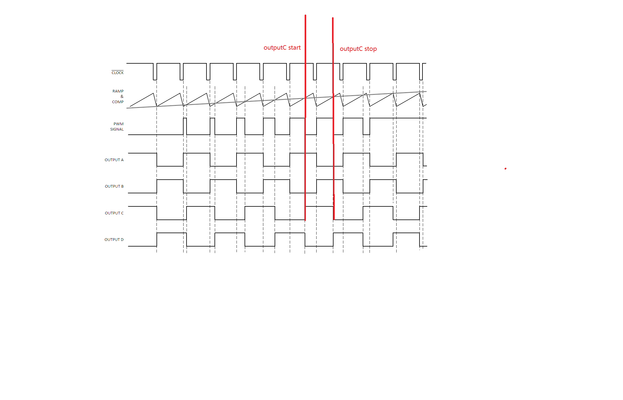
  • When we loaded around 300W( Output voltage 100V and input voltage 200V). Output is regulating at 100V noise is generating from the magnetic parts, while cross checking we observed asymmetrical pwm pulse output(between OUTC and OUTD). we work around as per the application note from TI SLUA275, but still issue not resolved. We increased Ramp voltage to 1.15Vdc by adding voltage divider from Vref output.
  • We tried with compensation circuit still issue not resolved.

We are using a four layer PCB for UCC3895 (as a separate daughter card) separate from power PCB. And a dedicated ground layer given for the IC,  but power ground and analog ground not separated which is common as ground plane.

Please help us to resolve the issue

  • Hi Arun, an expert will get to you soon. ——Teng

  • Dear TI Team

    please provide a reply

  •  Hi Arun,

    1, ,Do you check your signal that is there any interference signal on the Driver circuit.

    2, Could you please show your waveform here.

    thanks

  • Dear TI Team

    We are observing same waveform on input of the driver and output of the driver.

    We are attaching a waveform of OUTC from the PWM controller.

  • HI Dear,

     1,Do the OUTA and OUTB have same issue or not?

    2,could you please share you SCH in here?

    3,Can you please share OUTA OUTB OUTC OUTD in same waveform?

    4, Do you choose  Voltage-Mode or Peak Current-Mode?

    thanks

  • Dear Bliss

     1,Do the OUTA and OUTB have same issue or not?

    A:- NO issue observed

    2,could you please share you SCH in here?

    A:- Attached schematic

    3,Can you please share OUTA OUTB OUTC OUTD in same waveform?

    A:-Attached Waveform

    4, Do you choose  Voltage-Mode or Peak Current-Mode

    A:-There is no information on datasheet for 3895 how to operate in voltage mode or current mode. Any way we connected Resistor from Vref to Ramp pin and capacitor from same pin, along with a resistor connected to CS pin as per work around done given by SLUA275.

    5367.files.zip

  • Hi Sarma,

    I am happy hear from you.

    as my attach waveform from datasheet. OUTPUT-C start and stop,it is closely related to RAMP and COMP.

    so, some suggestion for you.

    1, you need to check the comp signal is stable or unstable.

    2. your RAMP from CT,

    a, you need to check this signal is clear or not.   for your waveform OUTA, there is strong interference signal. it may cause distortion of CT current signal detection.You can try filter the current signal appropriately, but it may not be effective.

    b, I think you need to add Slope compensation on RAMP PIN. please refence http://www.ti.com/lit/ug/sluu109b/sluu109b.pdf

    c, for got stable CT current signal, I suggest you put you CT on the input Bus. please refence http://www.ti.com/lit/ug/sluu109b/sluu109b.pdf

    3,  what is the value of R55 R56 R57 R58? these Resistors should be 10K.


  • Dear Bliss

    We have checked Ramp and comp pin wave forms please find the waveform attached. Please check and provide your comments.

    We have given slope compensation as per the application note which is already incorporated in schematic which previously shared.

    We connected CT on the Input bias but not observed any improvement.

    R55 to R58 are 120 Ohm resistor, we are using SIC mosfet as switch, for that purpose we are using driver IC from power integration part # SID1182K. This IC will receive logic input 3V as high and 0V as low. if we are giving more voltage input it will shutdown pulses. Our PWM controller output is 12 Vpeak, so we are dividing 12V with voltage divider and given to mosfet driver. 8562.waveform.zip

  • Hi Arun,

    1,I reviewed your waveform.  It seem that there is significant interference on the Ramp signal. I just put good Ramp Signal at here for reference.

    2, for  slope compensation, I put the Key circuit for you. there is no R3 in your SCH.

    3,R55 to R58 are 120 Ohm resistor, could you please change R55 to 1.2K (R42 to 3.3K)  to reduce the IC lose.

    4, Do you try change the dead time? increase or decrease.


  • Dear Bliss

    we cannot able to resolve the issue, we thought that this due to current mode control. please provide information how to operate this controller on voltage mode. we need circuit diagram for voltage mode configuration of UCC3895

  • Dear Bliss

    we cannot able to resolve the issue, we thought that this due to current mode control. please provide information how to operate this controller on voltage mode. we need circuit diagram for voltage mode configuration of UCC3895

  • Dear Arun,

    I am looking for the answer you want. I will reply you later.

    thanks

  • Hi Arun,


    UCC3895 in Voltage Mode control. The figure do not show the secondary side error amplifier (TL431), loop compensation or opto-isolator circuits. you need to design it by yourself.

    1,A DC blocking capacitor to the primary of the transformer – this is necessary in VMC.

    2,Q1  provide a slope compensation ramp – this is used ONLY when the system is in current limit and may be omitted if the designer can accept sub-harmonic oscillations in current overload conditions.

    3,Please calculate component values by yourself.


  • Dear Bliss

    Thanks for your support, now issue resolved.

    Regards

    Arun