This thread has been locked.

If you have a related question, please click the "Ask a related question" button in the top right corner. The newly created question will be automatically linked to this question.

TPS65023B: Is it OK to back drive the VDCDC# pin?

Part Number: TPS65023B

Hello,

We're reusing our TPS65023B PMIC circuit to power noise sensitive circuitry, so we want to give ourselves the option to use a bench top supply for one or more rails. 

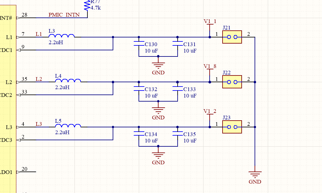
Please see included schematic. 

Is it OK if we use a bench top supply for one of the jumpers and pull the inductor (e.g., apply 1.1V to J21 and pull L3)?  Should we also disable the DCDC#_EN in this case?  

Any guidance or concerns that you can provide will be appreciated.

Thank you,

Bob

  • Hi, Bob,

      Thank you for using TI PMIC in your design! since you're powering noise sensitive circuitry, as an option to check if TI PMIC is good enough for your application, its better to separate the DC/DC output (it's also recommended to disable the DC/DC) from the noise sensitive circuitry by a jumper and applying a bench top supply to the other pin of the jumper.

      FYI, all 3 jumpers in current schematics can easily short the output DC power supplies to GND by mistake; reconnecting them between load and PMIC DC outputs can separate the load from DC/DC outputs.

      The device expert will be back from vacation soon; he may give you more detail recommendation. 


  • Bob,

    If you lift the inductor, then there is no way for current to go through the device and out of the L1/L2/L3 pins. The voltage on these Lx pins doesn't matter because they are isolated from the load (V1_x). The voltage present on VDCDCx feedback pins will cause the pulse-width on L3 to change as the regulator switches, but it will not cause any issues. As long as the voltage applied at VDCDCx is within the Absolute Maximum Ratings, then it is unlikely that any damage will occur.

    As my colleague mentioned, it might be easier to just pull the DCDCx_EN (enable) pins to GND to disable the DC-DC regulator while you are performing your tests with the external power supply. This way, you don't have to worry about the Lx pin switching and possible generating noise that could be picked up in your measurements elsewhere on the PCB.