Because of the holidays, TI E2E™ design support forum responses will be delayed from Dec. 25 through Jan. 2. Thank you for your patience.

This thread has been locked.

If you have a related question, please click the "Ask a related question" button in the top right corner. The newly created question will be automatically linked to this question.

TPS73801: Remote sensing (Kelvin connection) during Ajustable operation

Part Number: TPS73801

Hello,

The TPS73801 can be used in 2 different mode: "Ajustable Operation" and "Fixed Operation".

In §7.3.2 (fixed operation), we can see "During fixed voltage operation, the FB pin can be used for a Kelvin connection if routed separately to the load."
In §7.3.1 (Ajustable Operation), we can't see anything about remote sensing.

I don't understand why Kelvin connection would be forbidden in Ajustable Operation.

Could you confirm that we can use Kelvin connection during Ajustable Operation?

Regards

  • Hi Sim2, 

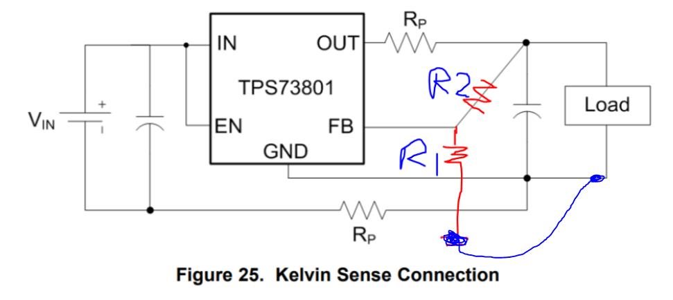
    You can still use Kelvin connection for the adjustable operation. Instead of having top resistor directly connecting to the Vout pin, you could have something like this which is simialr to the one discussed in 7.3.2 but with unity gain.

    Regards, 
    Jason Song

  • Hi Jason,
    Thanks for your help.

    As the GND track is routed to the load too, is there any special recommendations about stability in this operation mode?

    Additionaly, the SOT23 package exhibites 2 GND pins.

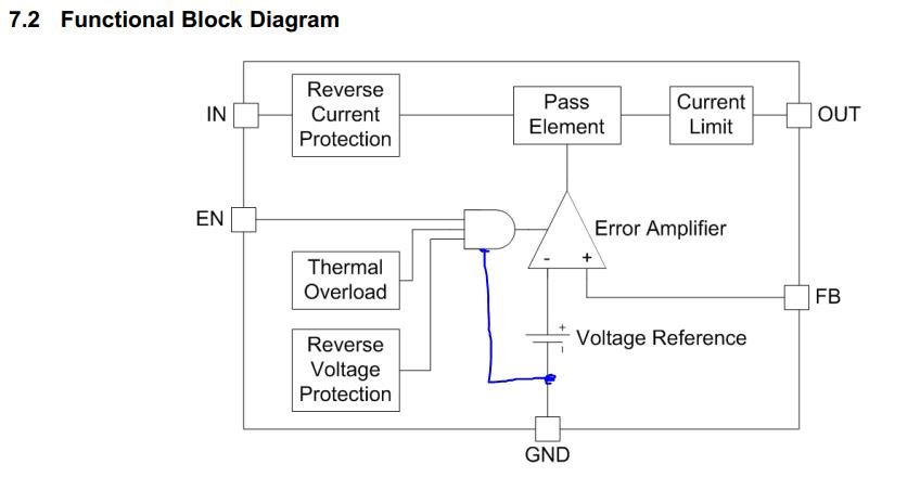
    From the functional block diagram the first one seems to be more a "FB minus" to sense the output voltage in differential with the FB pin .
    Could you confirm that no current flows throught it?

    Regards

  • Hi Sim2, 

    For stability, you need to make sure that the output capacitor is as close to the output pin as possible. Per datasheet, a minimum output capacitor of 10 μF with an ESR of 3 Ω or less is recommended to prevent oscillations.

    For the two ground pins, normally we would recommend covering both pins with a ground plane. Datasheet actually has a recommended layout example for you to reference. If you would like to use Kelvin connections, you may change the bottom side of R2 (circled in blue) close to the point of your load. 

    From the functional block diagram the first one seems to be more a "FB minus" to sense the output voltage in differential with the FB pin .
    Could you confirm that no current flows throught it?

    --I am not sure if I understand your questions, are you asking the current flowing through the resistor dividers? 

    Regards, 
    Jason Song

  • Hi Jason,

    Sorry for my unclear question. I will ask in an other way.

    Which of the 2 solutions is the right one?

    First solution:

    In this solution, resistors R1 R2 are connected directly to the load. The voltage drop across the 2 Rps is well measured so it can be compensated.

    But the ground of the TPS73801 becomes higher with higher load current and can be very different of Vin-.

    It seems to be a bad idea for EN internal logic:


    Second one:

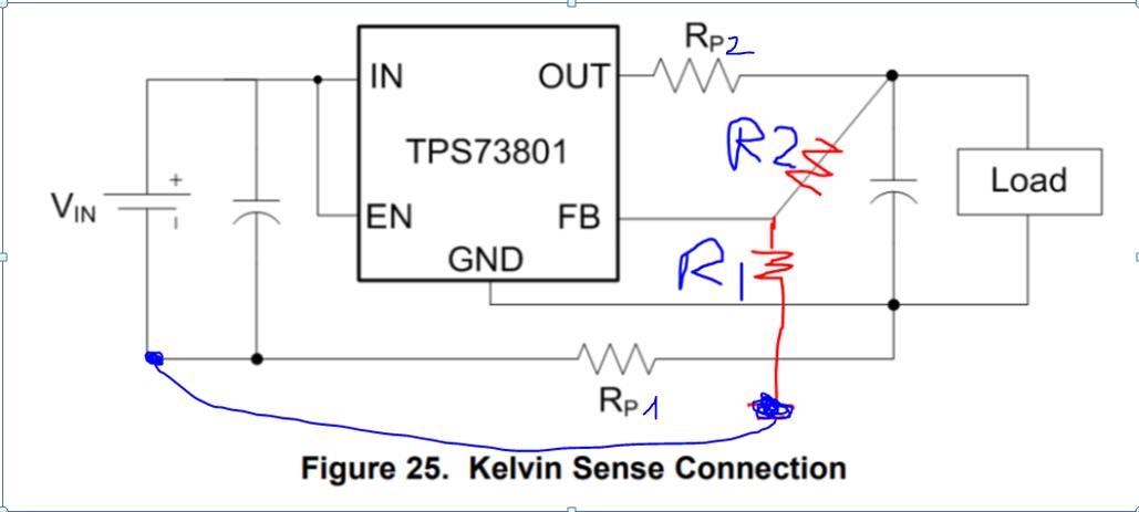
    In this way, the ground of the circuit is Vin-. It seems to be OK for the EN logic.
    But the voltage drop across Rp1 isn’t compensated :'(

    Regards,


  • Hi Sim2,

    For solution 1, I agree with your analysis, but I would not worry too much about the EN logics, the typical numbers for EN to be on is 0.9. Figure 11, 12 can give you the enable thresholds over temp. However, if EN logics are your concern, you should estimate the voltage difference on the ground of the LDO and the Vin-.

    For solution 2, the ground of the LDO should be Vin- + IgroundxRp1; here Iground is in the rage of a few milli-amps, as shown in Figure 7. Again, the device between Vin- and the ground of the LDO is not much. Essentially, the ground side of the FB resistor R1 is having a voltage potential difference of IloadxRp1 comparing to the output ground of the LDO and the load ground. But we only care about the potential at load input and load ground, this voltage will be increased to (1+R1/R2) x (Vref + IgroundxRp1). It will be higher than what we want it to be. 

    Unlike the signal traces from the output of the LDO to the input of the Load, normally, on a PCB, there will be a dedicated ground plane or at least a big piece of metal serving as a ground plane. The Rp1 drop from the load ground to the Vin- could be very small and can be neglected.

    If there is no ground plane and Rp1 is significant. I would recommend going with solution 1 that has the ground side of your FB as close to the ground of the load as possible.

    Regards,
    Jason Song