Other Parts Discussed in Thread: TPS7A05, TPS7A16
In the LM9076 Datasheet on page 10, "OUTPUT CAPACITOR" section, the first paragraph says the following:
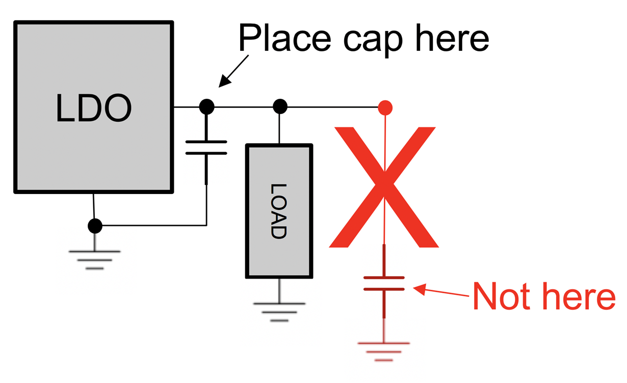
An output bypass capacitor is required for stability. This capacitance must be placed between the LM9076 VOUTpin and Ground pin, as close as is physically possible, using traces that are not part of the load current path.
QUESTION: How can you avoid using the Vout trace, through which "load current" flows? Vout is the "load current path." For that reason, I don't understand the meaning of the text above. Do you have an example PCB or can you otherwise explain "traces other than the load current path"?
Thank you.


