Hi,
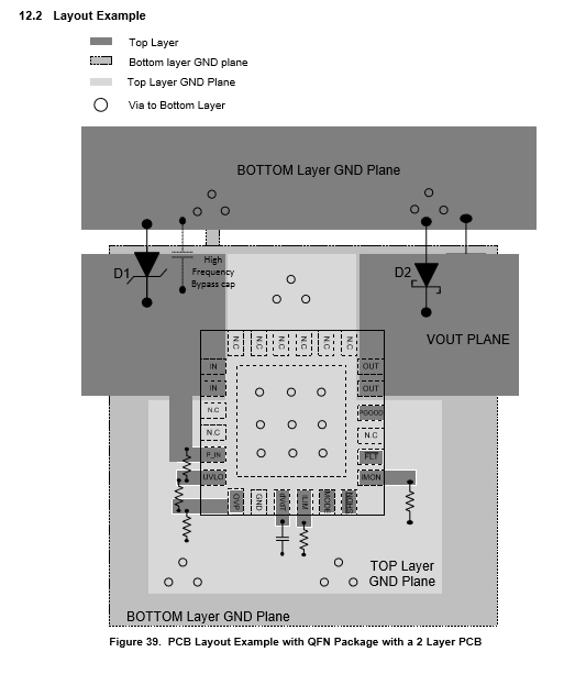
I'm designing a PCB based on TPS16630REG IC. According to the datasheet, it mention the IC ground connection is on TOP layer and high frequency bypass Cap in on the GROUND layer. Is it ok I route all component on TOP layer and connect the both layers using via?