This thread has been locked.

If you have a related question, please click the "Ask a related question" button in the top right corner. The newly created question will be automatically linked to this question.

UCC21750: How to decide the capacitor (CBLK) and resistor (R) for the DESAT function?

Part Number: UCC21750

Hi,

This gate driver is used to drive a SiC MOSFET, FF23MR12W1M1P.

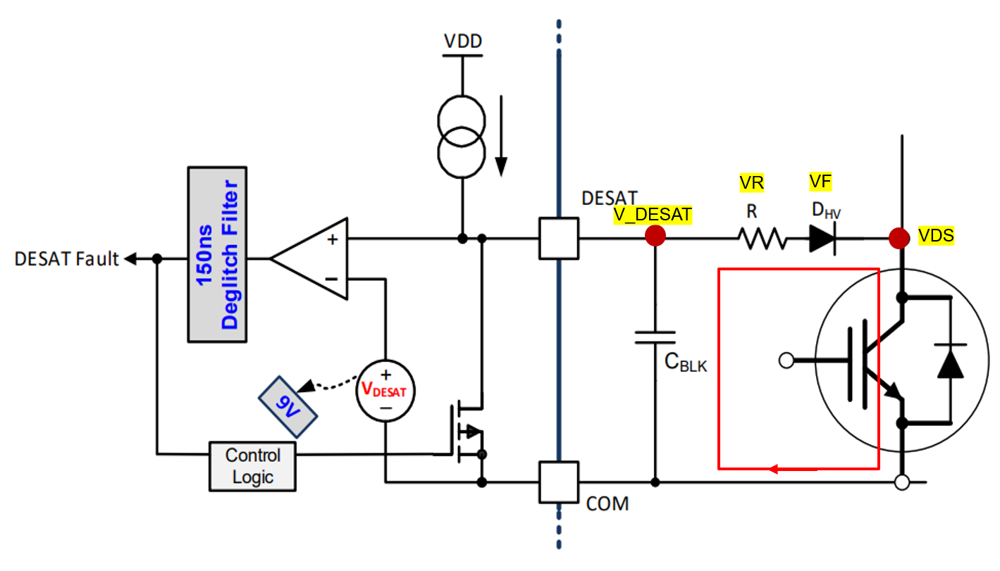
Could you please advise how to choose the capacitor  and the resistor for the denaturation function? This capacitor is called CBLK and the resistor is R on Figure 16 (page 22) of the UCC21750 datasheet.

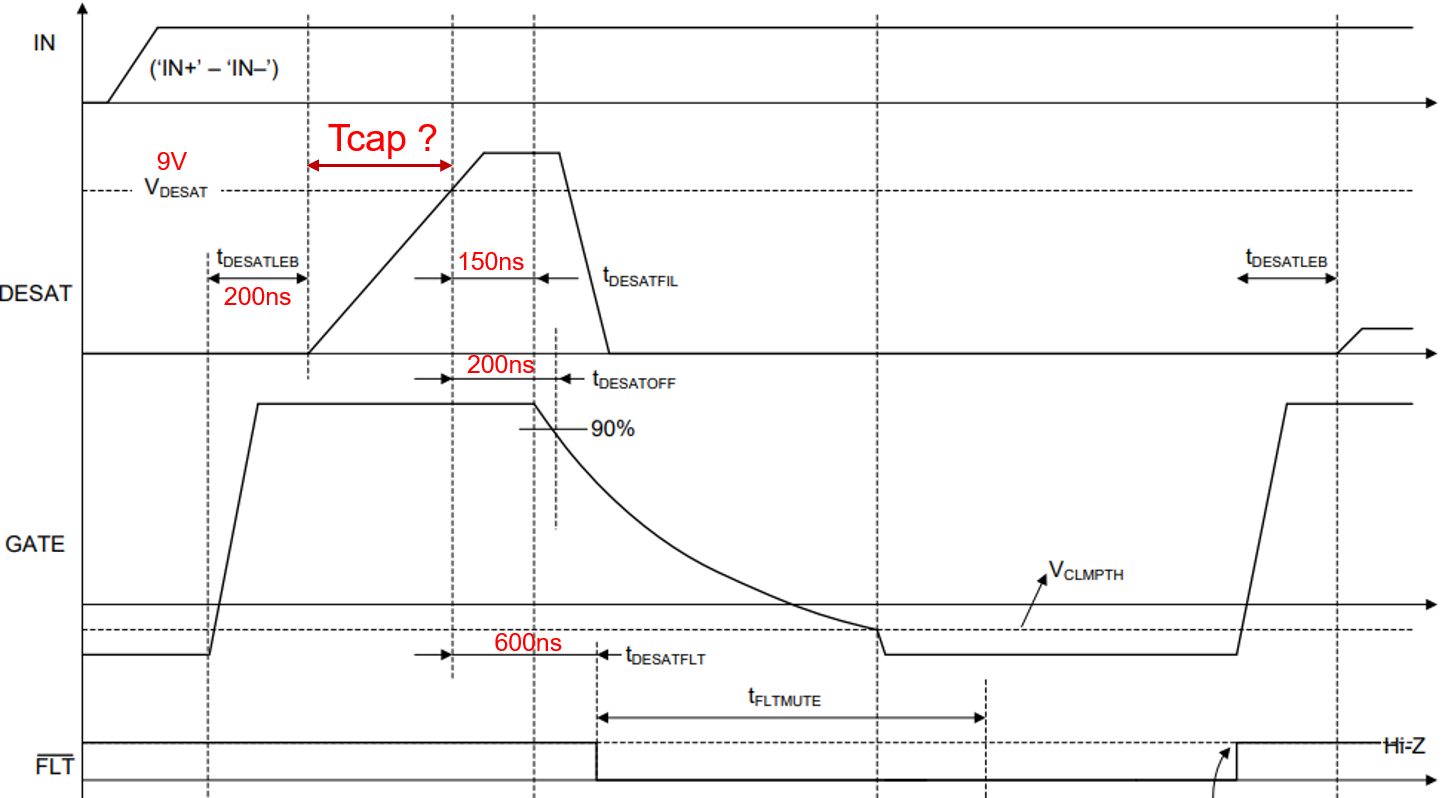
What is the best for Tcap in the following figure? 

According to SLUA863A, Tcap=Vdesat*Cblk/Ichg=9V*Cblk/0.5mA;  If Cblk=50pF, Tcap=900ns, so the total time from denaturation detection to fault is 900ns+600ns=1.5us. I am not sure if my calculation is right? Do I need to consider anything else?

then how to decide the R? 

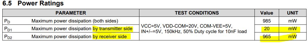
Another question is to help understand 6.5 power ratings on page 5.

Does this transmitter side mean the low voltage side (VCC side, pin 9-16) and the receiver side mean the high voltage side (VDD side, pin 1-8)? 

Thanks,

Hongmei

  • Hi Hongmei,

    Thanks for your questions! You are correct that the blanking time is calculated based on t_BLK = V_DESAT*C_BLK/I_CHG. You may also consider the diode, DHV, and resistor, R, from Figure 16 which are connected to the drain of the SiC MOSFET. Based on the forward voltage drop, VF of DHV, and the voltage drop across R, R*I_CHG, then the DESAT detection voltage is reduced where V_DESAT,actual = V_DESAT - VF - R*I_CHG. Thus, the t_BLK will be smaller than you have calculated. 

    Additionally, the total time until the fault is detected will be t_BLK+t_DESATOFF, which in your example would be 900ns+200ns = 1.1 us. This is because the driver takes action after t_DESATOFF to begin to shut down the SiC MOSFET, while t_DESATFLT is the time it takes for the driver to send a signal to the nFLT pin.

    To answer your second question: yes, the transmitter side is the low-voltage VCC side and the receiver side is the high-voltage VDD side, as you mentioned.

    Regards,

    Audrey

  • Hi Audrey,

    Thank you very much. I am still kind of confused.

    V_DSET:  pin DESAT voltage, reference to COM in the figure, actually is the voltage across the CBLK.

    VDS: device drain to source voltage, reference to COM in the figure.

    VR: voltage across the resistor 

    VF: diode forward voltage.

    When V_DESAT < 9V, normal operation. The CBLK should be charged to whatever it is ( VR+VF+VDS).

    When V_DESAT > 9V, desaturation is detected. To detect the desaturation, the CBLK should be charged to 9V. So in this formula:  t_BLK = V_DESAT*C_BLK/I_CHG, V_DESAT is 9V.  Why it is: V_DESAT,actual = V_DESAT - VF - R*I_CHG?

    Thanks,

    Hongmei

  • Hi Hongmei,

    When the IGBT is turned on, and is operating in the normal condition (no short circuit), VCE (or VDS as you show) is smaller than V_DESAT, so V_DESAT remains at VDS. 

    When the IGBT is saturated, then VDS > V_DESAT. Now I_CHG flows through C_BLK and the voltage is V_DESAT = VR+VF+VDS. From the standpoint of the IGBT, the value of VDS which trips the short-circuit protection is VDS = V_DESAT-VR-VF.

    Regards,

    Audrey