This thread has been locked.

If you have a related question, please click the "Ask a related question" button in the top right corner. The newly created question will be automatically linked to this question.

LM5116EVAL: Gate pulses are missing at certain load levels

Part Number: LM5116EVAL
Other Parts Discussed in Thread: LM5116

Hello,

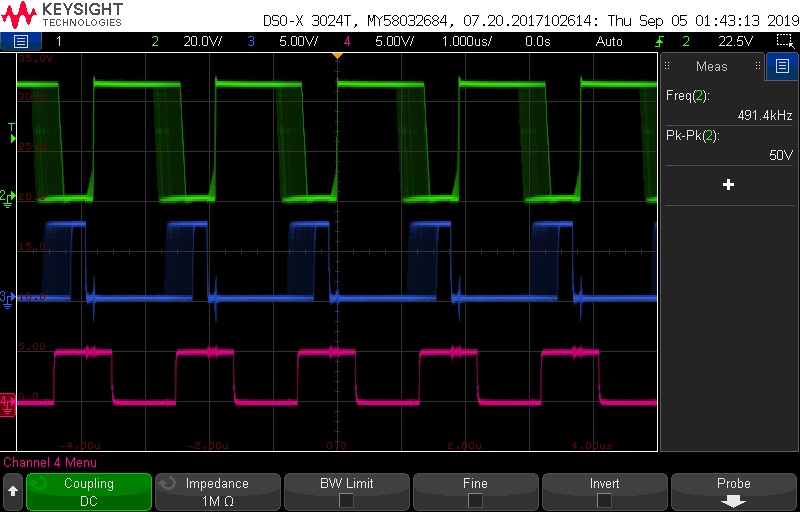
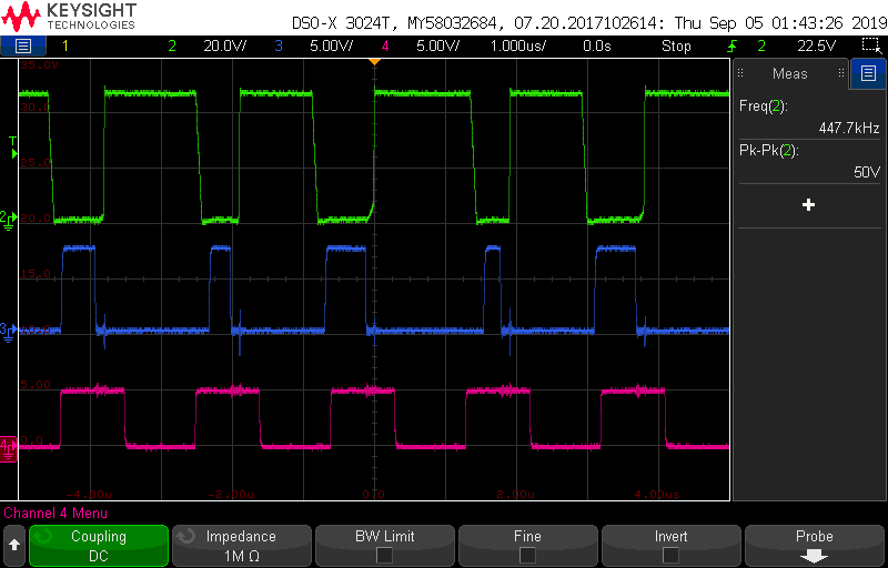
We are using an LM5116 in a 48v to 28v (2A max) SMPS design.  Under certain load conditions (~150-300mA) the circuit seems to become unstable and can often cause the low-side FET to fail.  We suspected our layout might be the culprit, but we were able to reproduce the issue using the LM5116EVAL board.   Any idea what may be causing this to occur?

Thanks....Alan

Small video link

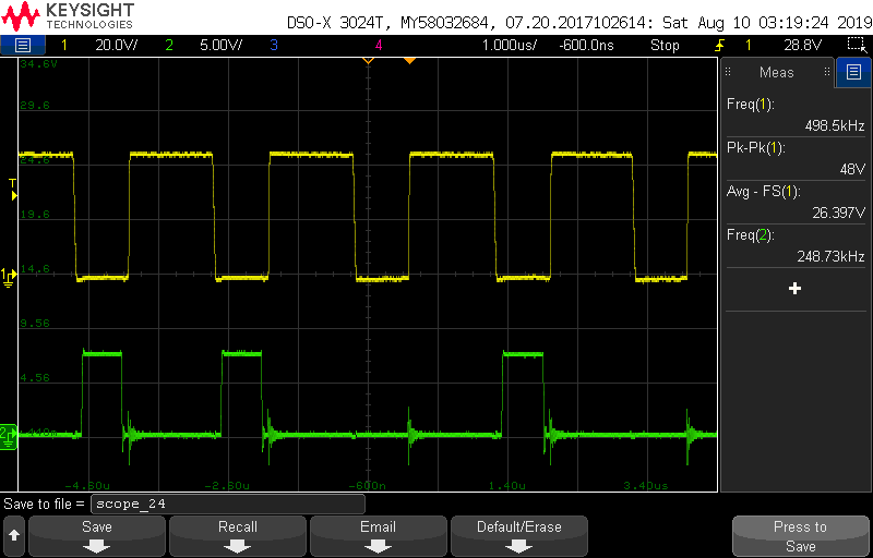
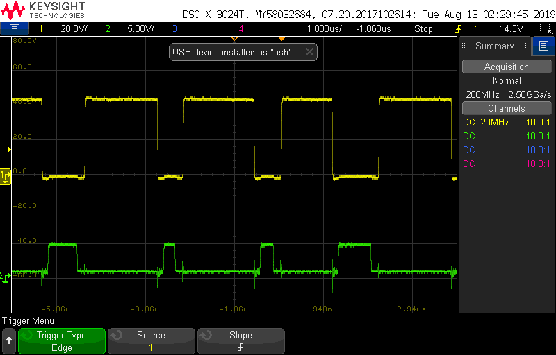
Yellow:  Inductor input voltage

Green: Lower FET gate drive

  • Hi Alan,

    Please send the schematic and a completed LM5116 quickstart calculator file so we can review component selection. I can also review the layout.

    Regards,

    Tim

  • Hi Tim -Thanks for responding to my question!

    Update:  I was able to resolve the missing gate pulse issue by reducing the sw inductor to 15uH -but am not sure why this helped.  The ckt behavior is MUCH improved, but still a little quirky (see below).  

    Schem, Webench  report and Quickstart are attached.

    Thanks!.....Alan

    LM5116_quickstart_28V_spreadsheet.xls48 to 28v Design.pdfSMPS schem..pdf

    Yellow:  Inductor/switch voltage

    Green: Lower FET gate drive

    Vin=44VDC, Load: 2.0A

  • Hi Alan,

    The looks like loop instability. I notice that the compensation values in the schematic are different than the quicktart. Maybe you can reduce R74 and increase C113 values.

    Also check the ESR of the 33uF/63V electrolytic output cap as this creates an ESR zero (that may also vary substantially over temperature depending on the behavior of the ESR). Note that the electrolytic doesn't provide much filtering at 500kHz, so you could change the 1uF/100V ceramic to a 10uF/50V cap.

    Regards,

    Tim

  • Hi Timothy,

    Changed  C113/C114, R74  to 2.6nF, 33p, 24K  quickstart values.  Also changed C45, 1uF/100V ceramic to a 10uF/50V cap (filtering seems ok, see below).  I also isolated/fly-wired the output inductor&cap onto the input cap to provide better/shorter ground paths.  Unfortunately, no stability improvement was obtained via any of these changes.  Any other suggestions?

    Thanks!.......Alan

  • HI Alan,

    Please send the layout for review. Also, can you send a waveform of the load transient response - that is a good indictor of stability.

    PS: that output ripple waveform looks stable.

    Regards,

    Tim

  • Hi Timothy,

    The transient response seems pretty good (see attached).  I sent you a link to the design files in a PM.  The output ripple appears stable cuz it was a one-shot capture.   

    Thanks for your assistance -much appreciated!.......Alan

    Loading = 0.5/1.0A

  • Hi Tim,

    Was wondering if you had any other suggestions concerning this issue?

    Thanks!......Alan

  • Hi Alan,

    What is the ESR of the output cap (as this sets an ESR zero)?

    Depending on the ESR zero, C114 of 300pF between COMP and FB in your original schematic seemed high as it sets a 15kHz pole when breaking with R74 (36.5k) compensation resistor. However, I see above you tried with different compensation values.

    Another recommendation is to add a small RC filter at the VIN pin of the IC (e.g. 10Ohms and 47nF/100V).

    In terns of layout, please ensure the current sense lines from the shunt to the controller are routed tightly and away from noisy nodes such as SW and LO (add a 50ns RC filter on the CS lines if needed). The feedback and compensation components should be close to their respective pins. Also, the ceramic input cap(s) should be as close as possible to the MOSFETs. More details are found in the layout section of the LM5116 datasheet.

    Regards,

    Tim 

  • Hi Alan,

    You might also check that the input filter is stable. The requirement is that the peak output impedance of the input filter is below the closed-loop input impedance of the converter. Thus, worst case is low Vin and full load.

    Damping is required and provided by the input electrolytic caps - just check that they have adequate ESR (you may have to add series resistance). See here for more detail: Simple solution for input filter stability issue in DC/DC converters

    Regards,

    Tim

  • Hi Tim,

    Argh!  Have been blowing up a lot of LM5116s and lower FETs while trying to solve this thing!

    Bad news: have tried most of your suggestions and nothing seems to improve the situation (haven't tried changing the input filter yet).  I thought changing the output inductor had solved the issue, but that verdict seems to have been premature.

    Good news (kinda): I think the issue is related to when the SMPS transitions from discontinuous to continuous mode.  At light loads, the ckt seems stable/normal.  As the load is increased, the gate pulses on the lower FET become erratic (some will be missing).  If allowed to run in this condition, eventually the the 5116 and/or lower FET will fail. At heavier loads, the operation becomes normal on the eval board, but is still somewhat erratic on our company design (see below).  This is a video that shows the situation (had to replace the lower FET shortly after this was shot). 

    Next, I think I'll try adding a snubber across the lower FET.  Hopefully the behavior described above will give you an idea how to cure this issue.

    Thanks!.......Alan

  • Hi Alan,

    Try running in FPWM mode. This maintains constant frequency across the full load range by allowing negative inductor current. See the description of the DEMB pin in the datasheet.

    Regards,
    Tim
  • Update:  After trying many things to correct the missing lower gate drive pulses , I tried switching the IC from diode emulation mode to fully synchronous mode.  This seems to have cured the missing gate drive issue that occurs when switching from DCM to CM modes.  I'm not really sure what the intended purpose of the DEMB pin is.  Can you explain?

    For the DEMB pin, the datasheet states: For start-up into a pre-biased load, tie this pin to ground at the CSG connection.  What is a "pre-biased load"?

    New Issue:  Now the supply seems to function mostly normally (still have some PWM irregularity, see pic above).  But when a 1.5 to 2A load is applied the lower FET and/or the 5116 will fail.  I've tried adding TVS diodes across its D-S and G-S pins.  Its an 80v FET.  The source voltage is 48V -maybe need higher rating?  FYI, we're using the same design, IC and FETs in a  48v to 12v design with no issues.  -This aspect made me heavily suspect these problems were layout-related -but I've tried many modifications that have not made any improvement.

    Belated answer to your previous question:  the output cap is: Panasonic 63SXV33, 33uF, 63v, ESR=25mohms.

    Thank you for your assistance....Alan

  • HI Alan,

    The function of the DEMB pin to allow diode emulation of the low-side FET, which allows DCM operation for improved efficiency at light loads. Pre-biased load occurs if there is a voltage on the output prior to startup. See section 7.4.1 of the datasheet for more detail.

    In your case, there may have been noise on the SW and DEMB lines to the controller affecting current sensing for diode emulation mode.

    In general, there should be no reason to clamp the gate drive to the FETs. The normal gate drive amplitude form the controller is effectively the VCC level (or the external VCC if an external bias rail is used), and this is well below the FET's max gate drive of 20V. In terms of the Vds voltage, there is a leading edge spike at high-side MOSFET turn on related to parasitic inductance of the switching loop. This is manageable if the spike is below the rating of the FET and controller. It is minimized by placing a ceramic cap, e.g. 10-100nF, extremely close to the FETs, thus reducing the switching power loop area.

    Regards,

    Tim

  • Hi Tim,

    Have replaced the switching FETs with 250v (vs 80v) devices.  Much less FET failures now.

    The circuit is still pretty erratic.  Seems to work ok otherwise, but would like to figure out what is causing the flaky behavior.  Its probably layout related, but....

    Tried different sync signal tests -with no improvement.  Tried on-board internal 5116 clock (no sync), PCB generated sync, sync via lab generator, various frequencies, duty cycles, magnitudes.

    Learned a couple minor things:  1) Circuit stops regulating (but looks stable) if sync duty cycle < 49%.  2) Certain sync freqs appear to stabilize the circuit, but it is load dependent. 

    Have run out of things to try, so will close this issue for now.  Will reopen if new questions arise.

    Thanks......Alan

    Green:  FET/Inductor waveform, Blue: Lower FET gate Drive, Pink: Sync

    Single shot of the above: