Other Parts Discussed in Thread: TPS24701,
Hi,
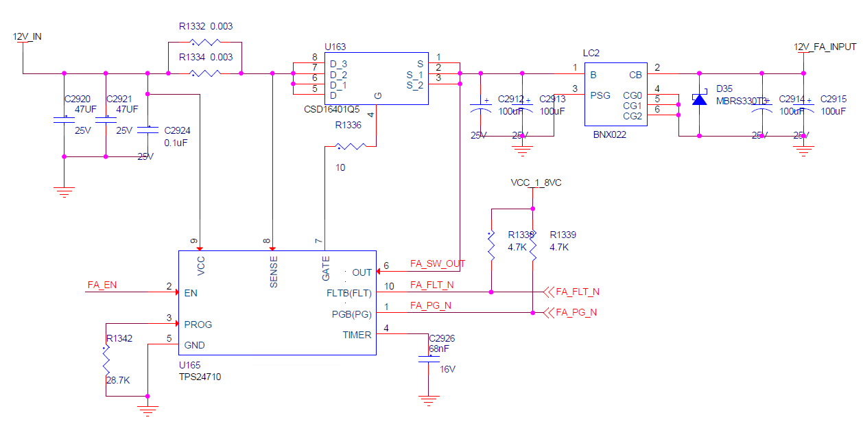
Following is the schematic of the power input circuit which uses TPS24701 as the hot swap controller.
the input voltage is 12VDC, and the max. current is about 15A-16A.
the design parameters in following figure is calculated according to the datasheet of TPS2471x.
Now, the Gate is always low after power on.
The voltage of EN pin is about 1.5V.
the output of FLTB is low, and that of PGB is high.
the wave of the Timer pin is zigzag wave.
BNX022 is a LC filter.
Why is TPS24710 always in Latch mode (the wave of the Timer pin is zigzag wave)?
Thank you.