


Other Parts Discussed in Thread: UCD9090
Hello Team,
Our customer is trying to debug their dual phase buck solution using our TPS53647 controller and CSD95372 power stage. This is what they reported..
" I found in the 0.85V (Rail #1 in UCD9090) power supply a TON_MAX fault, which I expected but, also an UV fault and when I measured, I also found over 1 V output. Then I started to measure the PWM that go to the CSD95372 ICs and the enable signal from the UCD9090.
There are two CSD95372 controlled by one TPS53647. One of them is not working properly as it does not perform switching.
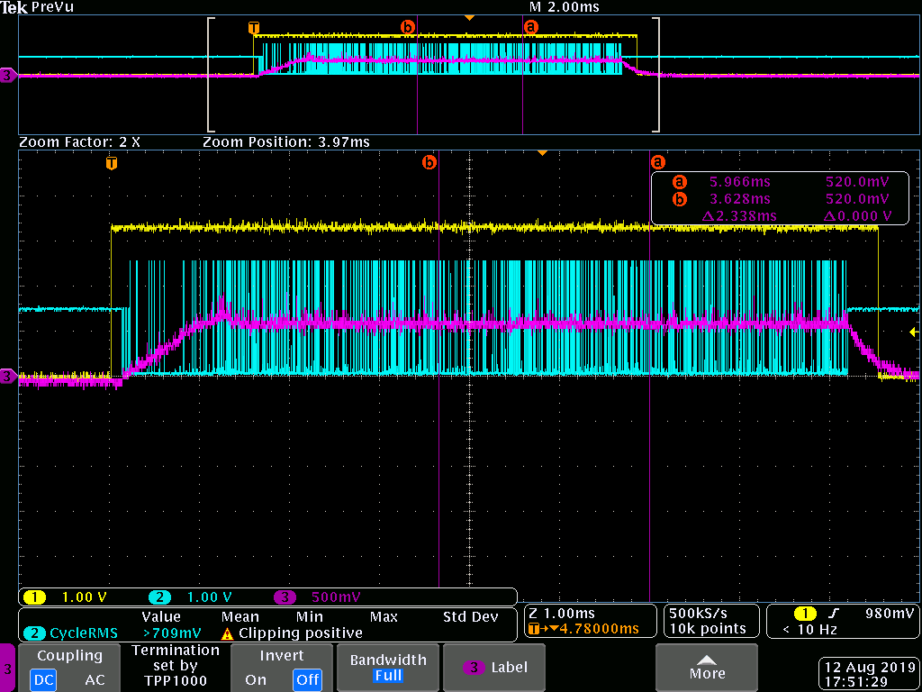
In the image “tek00215.png” it is shown a measurement of the enable signal from UCD9090 in CH1, the PWM signal is switching after the enable signal is ON in CH2 but latches, and in CH3 voltage keeps into an undervoltage condition and, as expected, drops after the PWM latches.
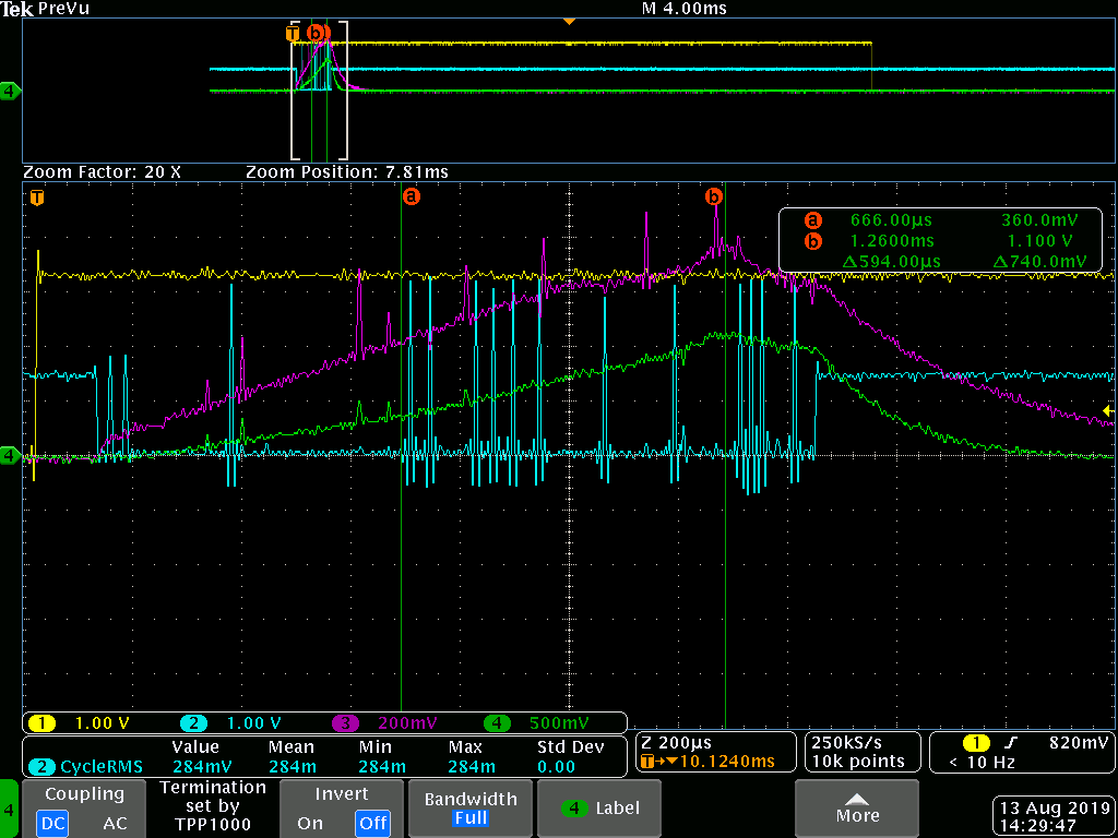
In contrast, “tek00218.png” shows a faster PWM shutdown. It was not able to replicate the same output voltage waveform, but IMON voltage is shown in CH4. The design have an RIMON of 190 kOhm, and reaching a voltage of 1.1V, it results into a current consumption of 40 Amps.
Can you help me answering the following questions?
- Under what conditions does the PWM can latch as in “tek00215.png?
- Is there a way to identify protection conditions? Like a pin that changed its state?
- Can I use the Fusion Digital Power Designer to visualize the registers within the TPS53647, through the UCD9090’s PMBus?


Please reach out to me to connect you to the customer directly if more sensitive information is needed.
Thanks very much,
Faizul Bacchus
