This thread has been locked.

If you have a related question, please click the "Ask a related question" button in the top right corner. The newly created question will be automatically linked to this question.

BQ76930: How does the cell balancing circuit work?

Part Number: BQ76930
Other Parts Discussed in Thread: TIDA-00449,

Hi

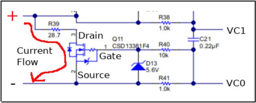
I'm using the reference circuit from TIDA-00449 and have a few questions I hope can be easily answered.  Please refer to the attached image I've created which shows the balancing circuit for a single cell.

What I understand is

a) The N channel MOSFET is turned on by the BQ76930 which enables current to flow from Drain to Source as shown in the image.  This allows the voltage of the cell to be lowered.

b) The resistor R39 is there to provide a load otherwise when the MOSFET turned on, it would result in a short-circuit (and damaged MOSFET)

c) The 10K resistor (R40) allows voltage to be applied to the MOSFET Gate but restricts current flow through the Gate - this is because MOSFETs are controlled by voltage not current.

What I do not understand and would like some help on is the following

a) What is the purpose of the 5.6V zener diode (D13)?

b) How does the BQ76930 turn on the MOSFET?  Is it via VC1 or VC0, since both are connected to the MOSFET Gate?

c) What is the purpose of the 0.22uF cap (C21)?

d) What is the purpose of the 1.0K resistor (R41)?

Thanks for any help on these questions.

Cheers,

Mike

  • Hi Mike,

    This app note will be able to help answer many of your questions since not all of this information is explained in the device datasheet: http://www.ti.com/lit/an/slua749a/slua749a.pdf

    Section 4 of the app note is on cell balancing and describes the purpose of the zener diode and how the BQ76930 turns on the FET

    The 1k resistor and 0.22uF cap form the input filter. This is also discussed briefly in Section 4 and the recommended range of values for these components is covered in the datasheet electrical table (Rc and Cc). 

    I hope this is helpful.

    Best regards,

    Matt

  • Hi Matt

    Thanks for pointing me to the app note.  It does help explain most of the questions I asked, however, I'm still not clear on how the external balancing FET is enabled.

    Matt Sunna said:

    Section 4 of the app note is on cell balancing and describes the purpose of the zener diode and how the BQ76930 turns on the FET

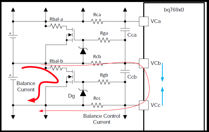
    This section describes a 'balance control current' and this is shown on the attached image (I copied from the app note).  What I'm still unclear on is

    a) why is there a balancing control current instead of a balancing control voltage?

    b) if I use the diagram showing the balancing control current, I still can't see how this affects the MOSFET gate voltage.

    b) which BQ76930 pin is responsible for controlling this current, VCc or VCb?

    Thanks for your patience Matt.

    Cheers,

    Mike

  • Hi Mike,

    The BQ76930 supports both internal balancing or external balancing (using the external FETs). With internal balancing, there are internal FETs that are switched on to connect VCb and VCc. This also operates the same way when the external components are connected. In this case VCb and VCc are internally connected which causes the voltage at Rgb to rise to turn on the FET.

    Matt

  • Thanks Matt, that helped clarify how the gate is controlled.

    Cheers,

    Mike