This thread has been locked.

If you have a related question, please click the "Ask a related question" button in the top right corner. The newly created question will be automatically linked to this question.

UCC27712: Path during HS and VDD

Part Number: UCC27712

Hi,

My customer is evaluating the UCC27712 on their board.

Then, VDD voltage seems to appear at HS node when HI and LI = Low condition is kept.

Does the UCC27712 have a path during HS and VDD?

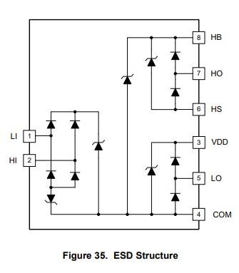
I guess that there is no path according to the following figure.

Best Regards,

Kuramochi

  • Hello Kuramochi,

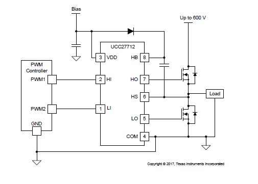
    Thank you for supporting the UCC27712 with your customer. Inside the IC there is not a path from VDD to HS. In the application circuit however there is a path. The bootstrap diode is connected to VDD and HB to charge the HB-HS capacitor. The current charging path is from VDD to the HB-HS capacitor so the HB capacitor charging current flows into HS. The HB-HS capacitor is charged by HS transitioning close to ground which is usually when the low side FET turns on. If both LO and HO are LO. The VDD to HB path thru the boot diode will raise the HS voltage if there is a high resistance from HS to ground.

    See the simple application below.

    Confirm if this addresses your questions or you can post additional questions on this thread.

    Regards, 

  • Richard-san,

    I have an additional question.

    We confirmed that VDD appears at HS even if boot capacitor is eliminated.

    So I guess that there is pass during HB and HS by protection diode.

    Do it have the path else?

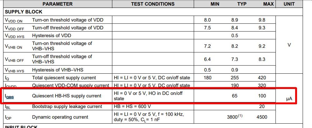
    Is "IQBS" related to?

    Best Regards,

    Kuramochi

  • Hello Kuramochi,

    The HB-HS quiescent current you highlighted on the datasheet is a current path that exists due to the HB to HS driver and level shifter circuits. Any ESD protection diode would not be an impact until higher voltage exists from HB-HS than the datasheet ratings.

    Confirm if this addresses your question, or you can post additional questions on this thread.

    Regards,