This thread has been locked.

If you have a related question, please click the "Ask a related question" button in the top right corner. The newly created question will be automatically linked to this question.

TPS43060 damaged in PWR ON/OFF test roud

Other Parts Discussed in Thread: TPS43060

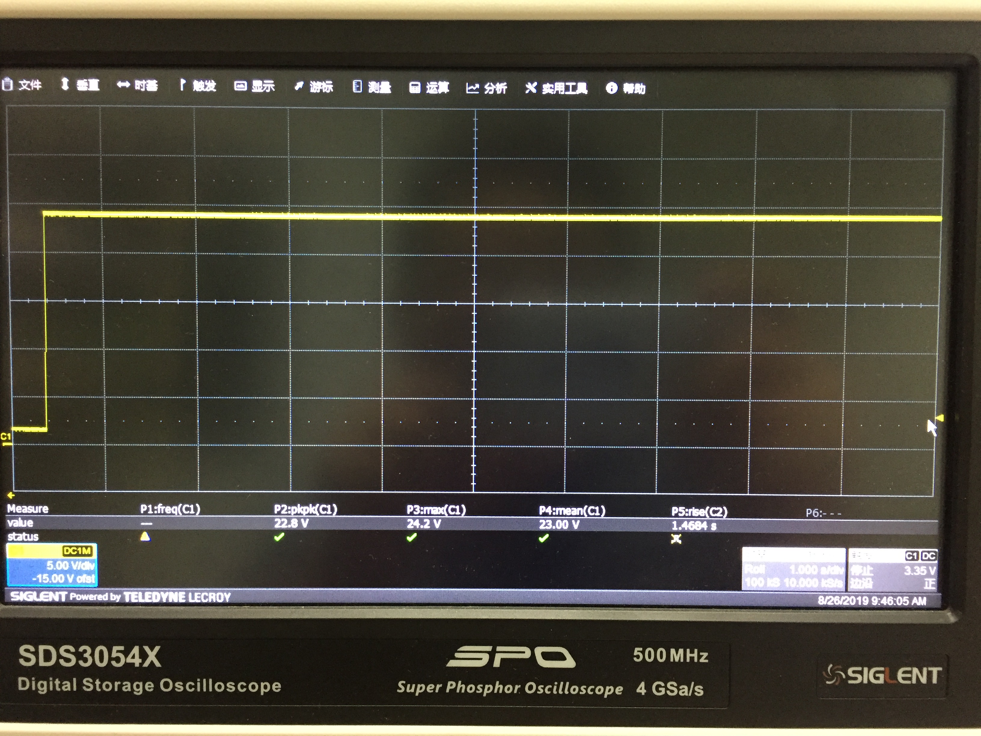
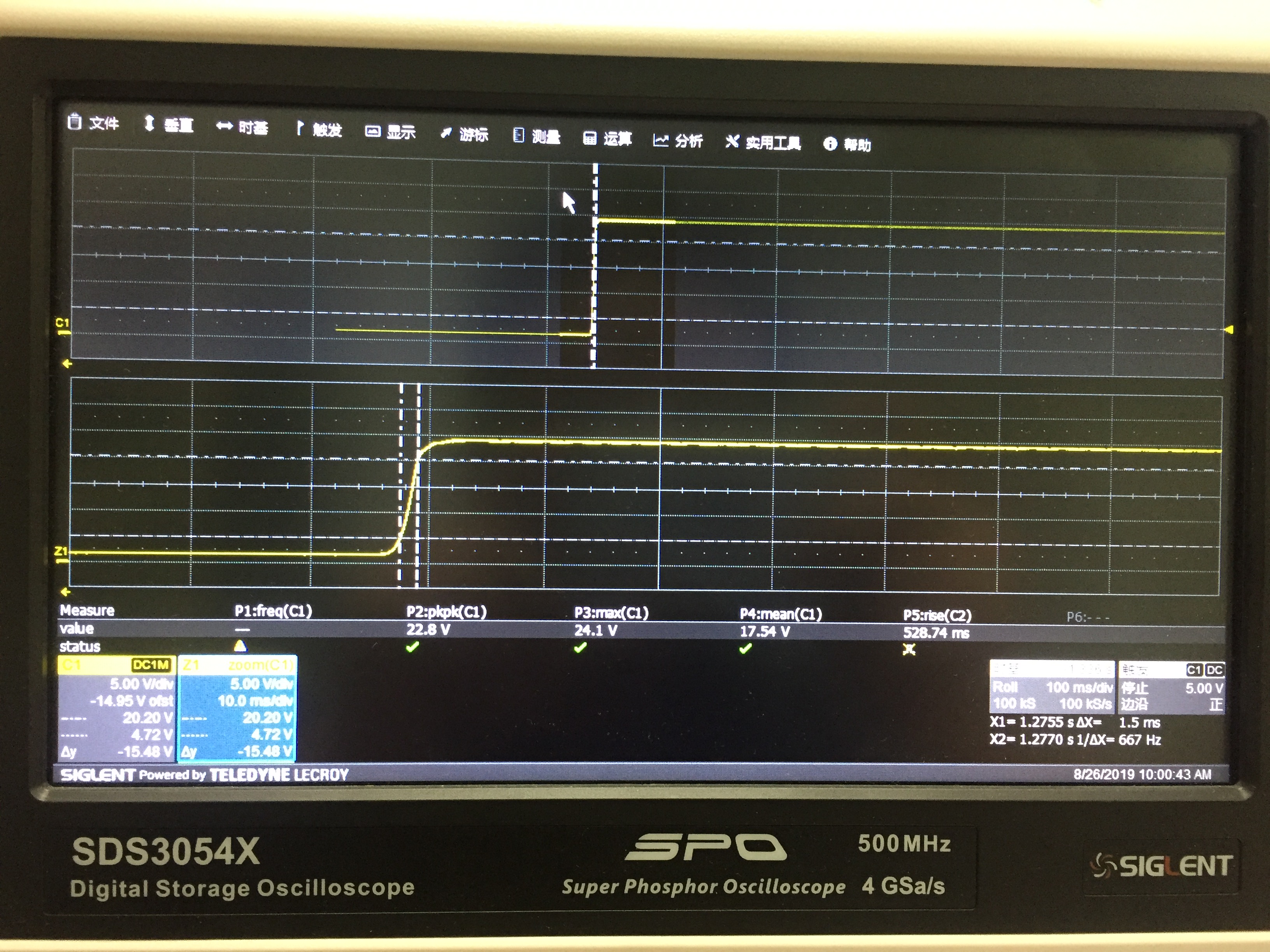
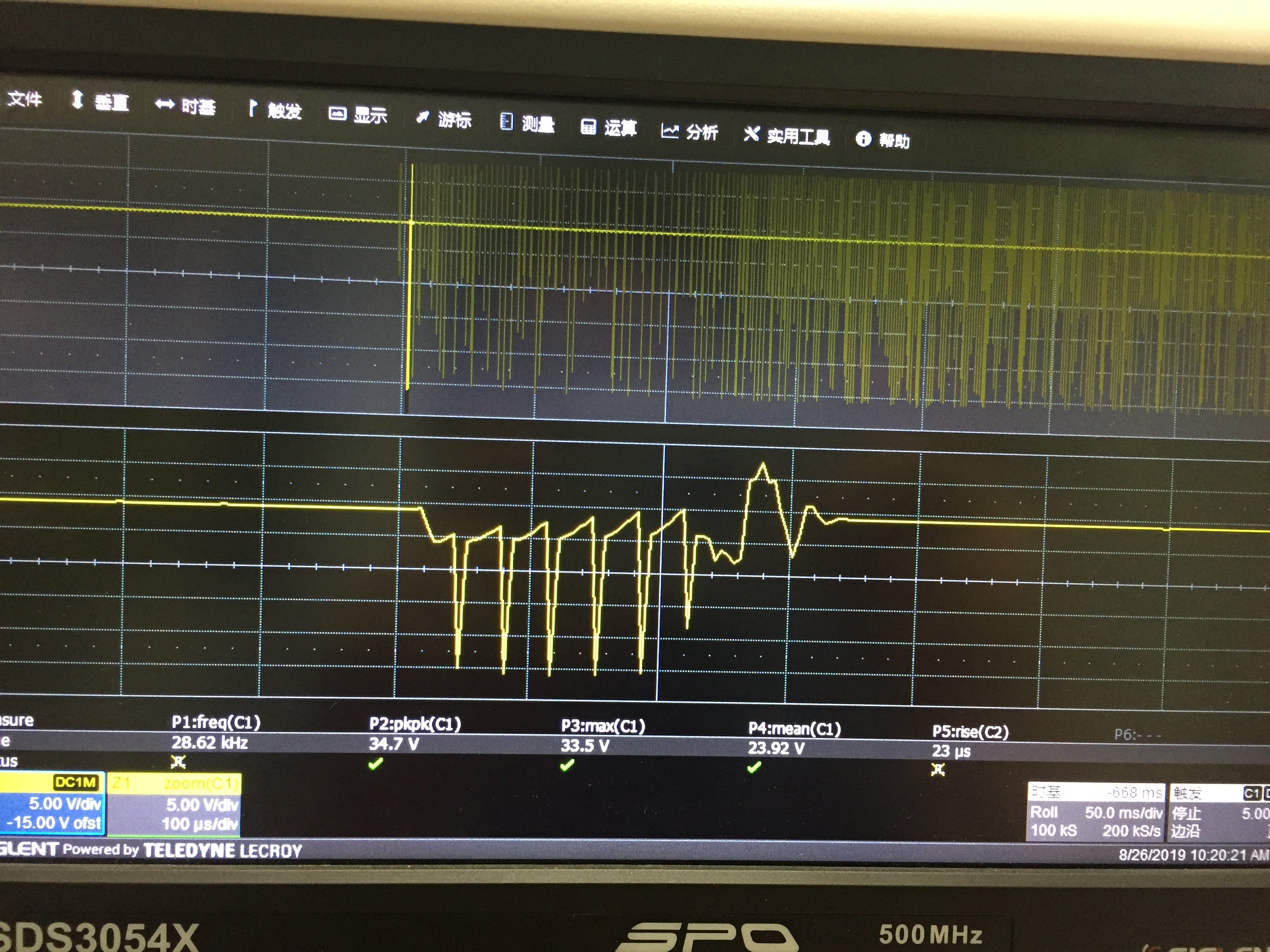
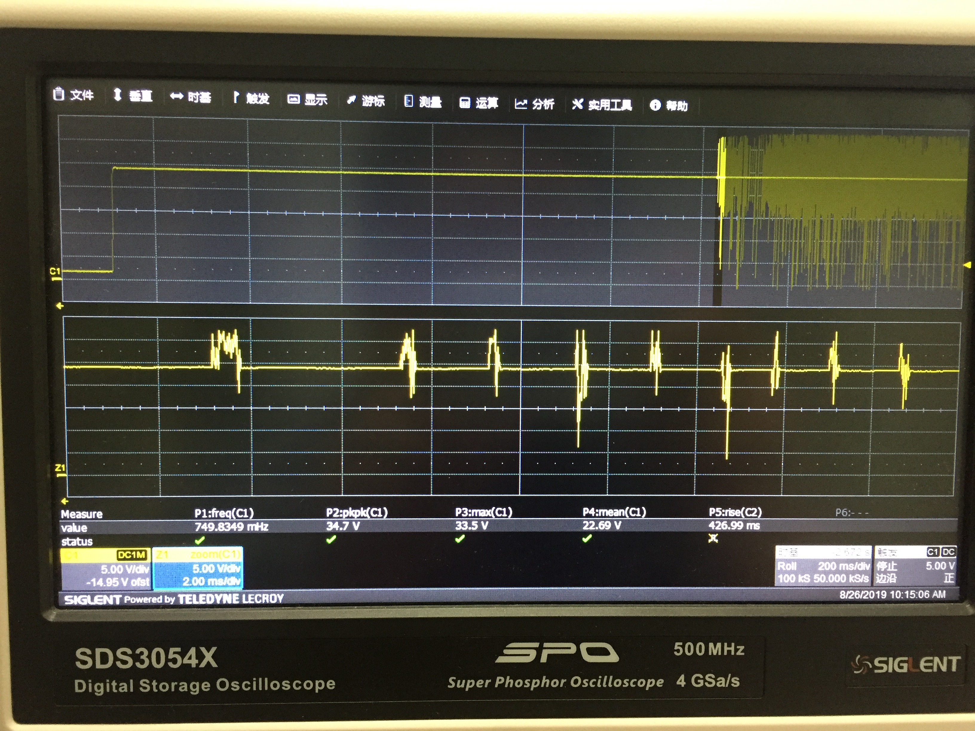
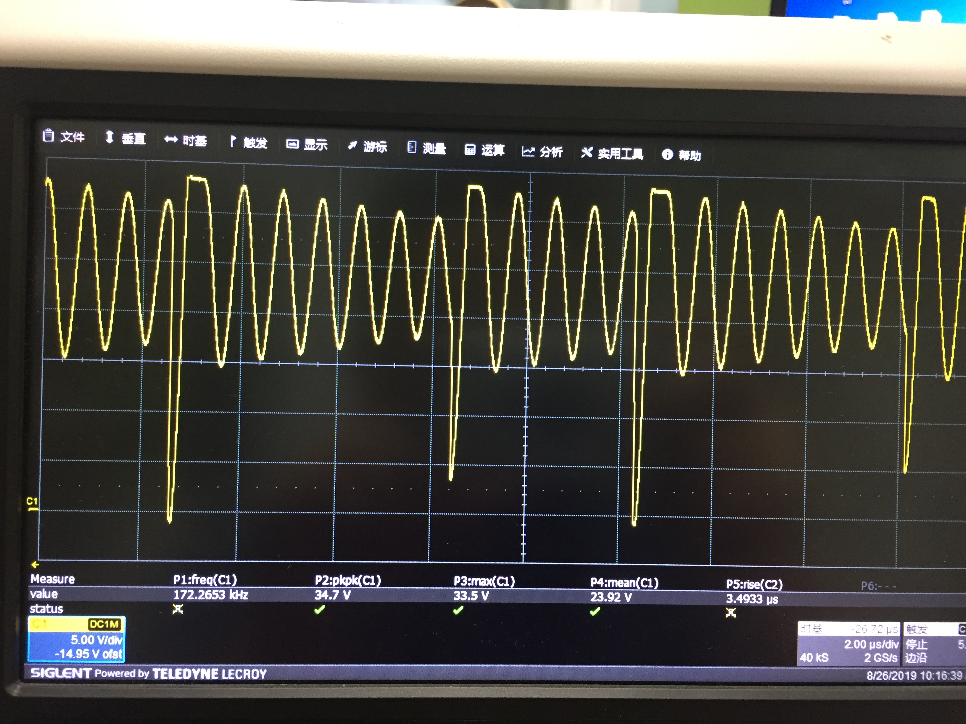
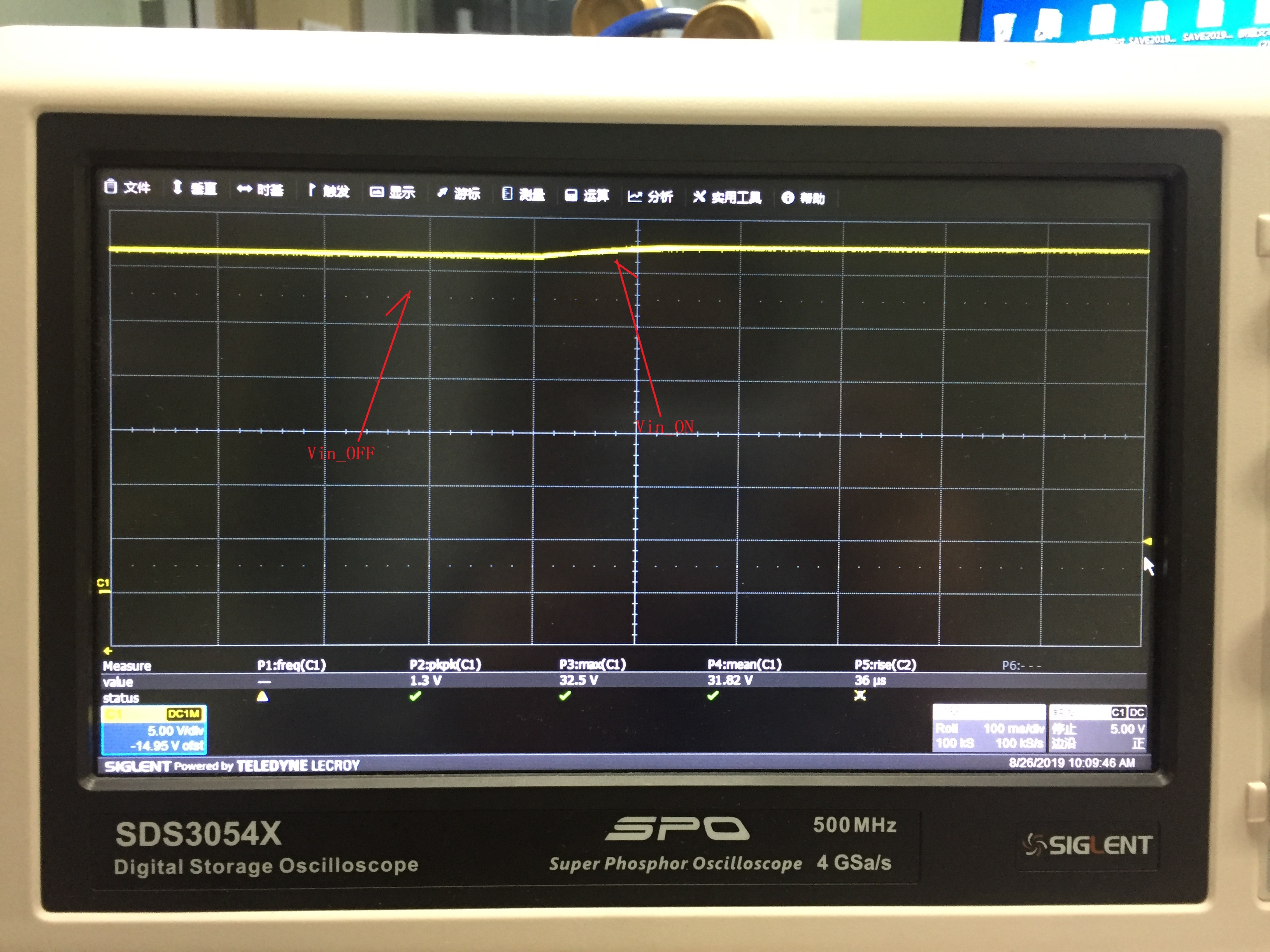
As attached, Vbus is the 24V DC_PWR in。During PWR ON/OFF test  ,the tps43060 will be damaged  after 1500 test round.
We wonder that if there is some advisement to solve this problem,TKS sincerelysys_attachment.pdf

  • Hello,

    Thank you for posting.  I thought I replied yesterday, but somehow my reply may not get through.  There no obvious clue in your schematic to tell how this happened.  To help us better understand the issue, could you send some key waveforms like the SW node, Vin and Vout during the PWR ON/OFF test.  Both overview and zoom in scope pictures are needed.

    Please also provide the following info: 

    • What is the input voltage slew rate during the test?
    • What is the load condition during the test?
    • What is the time interval for the ON, and OFF? 

    Thanks,

    Youhao Xi, Applications Engineering

  • Hi ,Youhao

    First of all,TKS for your attention.According to your suggestion,some key waveforms were captured.

    There is some info for your concern below:

    (1)As shown in the Input_Zoomin,the input voltage rise from 5V to 20V cost about 1.5ms.

    (2)During the test,The Vout was cut off by the MOSFET Q27,Thers is almost no load.And the quantity of electricity will be storaged by the Ultra-large capacity capacitor all the time.

    (3)During the test,the On-time was 46 seconds,and the Off-time was 6 seconds

    Thanks

    KeyWaveform.rar

  • Hi,

    Sorry I am not able to open the waveform file.  Could  you re-zip it so I can take a look?

    Thanks,

    Youhao

  • Hi,

    Sorry。

    I try it again,and paste the pic .

    8032.Desktop.rar

  • 24V DC   Input_Overview:

    Input_Zoomin:

    SW_Zoomin2 :

    SW_Zoomin1:

    SW_Zoomin3

    SW_Overview :

    Vout_Overview :

  • Hi,

    Thanks.  I am trying to understand these waveforms.  Why it is so noisy?  May I bother you to do the following tests:

    (1) startup by input voltage application.  I need to see at the time scale of 1ms/div.  Monitor Vin, Vout, and SW.  two waveforms, 0A and full load.

    (2) step load response.  After the circuit operate, please do the step load test, and let the load current to change from 0A to full load, and also 50% load to full load.  Make the step load 50% pulse width, namely high load for 5ms, and low load or no load for 5ms, repetitive.  Monitor Iout, Vin and Vout.  Scope time scale 5ms/div.  Vout signal ac coupling.

    Thanks,

    Youhao

  • Hi, any updated info? or I can assume the issue is resolved?  Let me close this thread here but you are welcome to re-open it by adding a new post with required info.

    Thanks,

    Youhao