This thread has been locked.

If you have a related question, please click the "Ask a related question" button in the top right corner. The newly created question will be automatically linked to this question.

TPS2373: Power management forum

Part Number: TPS2373
Other Parts Discussed in Thread: UCC2897A, PMP20541, TL431

Hi team,

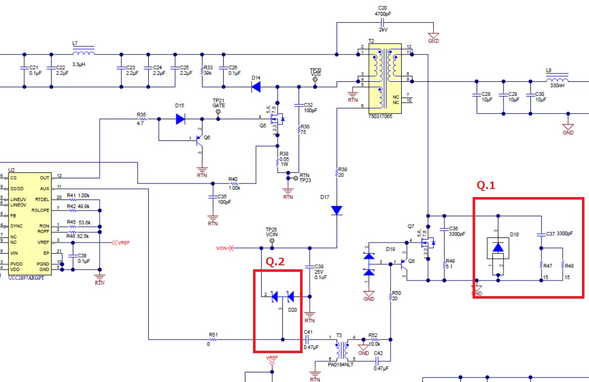
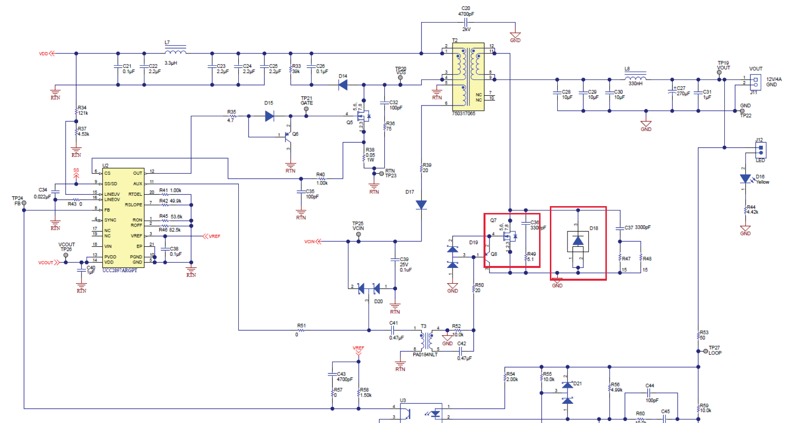
I have 2 question in 「TPS2373-3EVM-024 Schematic」.

①What's the purpose of D18,C37,R47,R48?
I think the snubber circuit is made up of C 36 and R 49. Is it a kind of snubber?
Please tell me this circuits purpose.Do you have any Design document?

②UCC2897A's Aux signal and VCIN singal are connected via D20.
What's the purpose of it?
Please tell me this circuits purpose.Do you have any Design document?

Thanks!

  • Hello,

    Thank you for your questions! You are correct in thinking D18,C37,R47,R48 is a snubber circuit. This circuit is used here in order to help with voltage and current spikes that happen during switching. This can help with ringing and therefore help EMI of the system. 

    D20 is used for transient and ESD protection. 

    Documentation can be found in the reference design library on ti.com:

    http://www.ti.com/tool/TIDA-050023

    Here you will find schematic and block diagrams, test data, design files and datasheets of the parts used. Please let us know if there is something specific you are looking for!

    Regards,

    Michael Pahl

  • Hello Michael,

    Thank you for your reply.
    I understood that This Schottky diode is to eliminate the body diode's contribution to the switch's behavior.
    I'll validate it with a test circuit.

    Regards.

  • Hello Michael,

    One more question.
    Is there waveform data showing the relationship between Q7 and D 18?
    It is the red square frame of the attachment.

    Regards.

  • Hello,

    A quick search showed me that we do not have a test report for that particular design at this time. I will check with a colleague to confirm. We do have a test report available for a design online that is very similar. The difference is that it does not include the pulse transformer or the FET. 

    In the link I gave above, there is a "Test Data" file to download. On page 12 it shows the switching waveform for D18.

    Regards,

    Michael Pahl 

  • Hi Michael,

    Thank you for your reply.
    If you find anything, please let me know.

    Regards,

  • Hello,

    I confirmed with a colleague that we do not have a test report for this design. The TI TIDA 050023 is the optimized solution: 

    Please note, as in my last message, that these are different designs. This design does not contain the FET you were asking about. If you want to look at a deisgn that does use that same topology, please refer to PMP20541: http://www.ti.com/tool/PMP20541

    You can compare the results for your question. Thank you!

    Regards,

    Michael Pahl 

  • Hi Michael,

    I have a question in 「TPS2373-3EVM-024 Schematic」.

    What's the purpose of R56  4.99kΩ?

  • Hello,

    R56 is used to bias the TL431 to give it about 2mA. Without R56, the current to bias TL431 (U4A) would need to come from the opto-coupler. Since this design is a 12V design and it uses a TL instead of a TLV, that current would be too high (we want to keep it around 5mA). Therefore, we use R56 to provide more current to TL431 so that it receives enough current to maintain high accuracy, without drawing too much current from the opto-coupler. 

    Additionally, since this is a different question about a different part from the original post, I would ask that you create a new thread. Thank you.

    Regards,

    Michael Pahl

  • Hello Michael,

    Thank you for your reply.

    I understand this matter.

    If I have different quetion about this,I will create a new thread.

    Regards.