This thread has been locked.

If you have a related question, please click the "Ask a related question" button in the top right corner. The newly created question will be automatically linked to this question.

Bidirectional DC-DC converter

Other Parts Discussed in Thread: LMR33620

Hi,

I want to find a bidirectional DC-DC converter with following requirements:

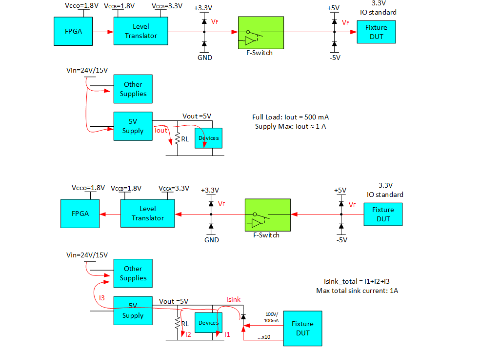
1: normal operation: 24V/15V to 5V/3.3V buck converter.

2: Sink current from output point: 5V/3.3V to 24V/15V. Max sink current is 1A.

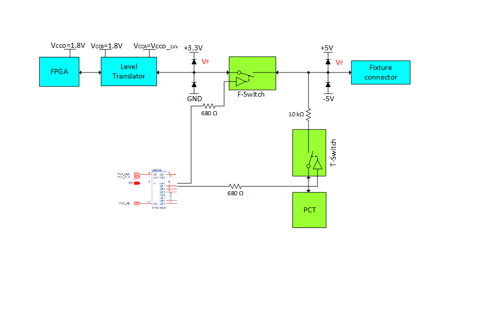
For example: IO protection

Due to the high speed IO >50MHz, series current limit resistor is not feasible. The fixture is connected to an unknown external DUT. The overvoltage and overcurrent is 100V and 100mA.

Thus, we consider to clamp the voltage by the external current limit of 100mA.

But this concept required a stable 5V and 3.3V power supply.

The supplies should be able to sink the current from the DUT. The worst case is 10 IOs are used at the same time, therefore a maximum sink current is 1A.

The load of the supplies is not enough to sink this current.

Do you have such a power supply that can be bidirectional to sink this current and match the above requirements?

  • What is the load current requirement for the two power rails (5V and 3.3V) in normal operation?

    "The overvoltage and overcurrent is 100V and 100mA"

    In reference the statement above, you expect the DUT's input who is connected to the DC/DC to rise above the regulated output voltage (up to possibly 100V) when the DC/DC needs to sink current?

    Sorry, but I am a little confused by the drawing. Could you highlight the inputs and outputs of both? DC/DCs?

    Thank you.

  • Hi,

    1: For normal operation: the load current requirements is 1A.

    2: The worst case of the unknown DUT is 100V and 100mA. It's possible up to 100V, but it also has an external current limit of 100mA.

        As you can find in the schematic, the IO voltage will be clamped by 5V+Vf, Vf is the clamping voltage of the diode (@100mA).

        The current will be absorbed to the devices and loads of 5V supplies. If the sink current is too high, it will charge up the +5V rail up to 100V.

        If we can absorbed this current, we can provide a stable +5V supply. And the IO voltage will be clamped at 6V to protect the 100V risk.

  • The current will be absorbed to the devices and loads of 5V supplies. If the sink current is too high, it will charge up the +5V rail up to 100V.

    • If the output can be clamped and you short the regulated output of the DC/DC to the DUT voltage, I could see a potential possibility of you biasing up that node and putting a lot of power through the HS FET diode. This could damage the HS FET diode possibly. Carefully consideration, would need to go into ensuring that the current is limited when this occurs. We cant guarantee that the HS FET diode could survive 80+ volts across it.

    There really isn't a spec in the datasheet for this, rather, this would be a fault condition that a buck converter can handle gracefully. It isn't normal datasheet operation for a buck converter to be a bi-directional device, though the FETs body diodes can conduct large currents for extended periods of time. This is something that we would not be able to characterize.

    LMR33620 would be an example device I suggest for you to sample and characterize its performance in your system.

  • Hi,

    1. As shown in the schematic, BAV99 is used. The current is limit by the external DUT given as 100mA. It can be a big voltage drop on the BAV99, but due to the current is only 100mA. the voltage will goes down quickly. There will be a spike when apply a 100V/100mA limitation input to the forward clamping circuit.

    2.If I am correct, buck converter can be used in a fault condition. Vout will be higher than Vin, and the current will go through FETs body diode. And I only need to design a 15V to 3.3V DC/DC, and make sure the body diode can handle enough current.

    3.Can I add external Schottky diode between the VIN and SW, maybe more to make sure the current from the Vout can be discharge to VIN?

  • 3.Can I add external Schottky diode between the VIN and SW, maybe more to make sure the current from the Vout can be discharge to VIN?

    Yes, just make sure it fits the application for power and speed.

    Best of luck. 

  • Hi Marshall,

    Please check the following information.

    1. For synchronous BUCK converter used in FCCM, the inductor will be negative for light load.

        LMR33620 has the PFM function, I think this cannot used to sink the current from the BUCK output voltage node.

    2. If I want to use a synchronous BUCK converter in FCCM, the negative inductor current will go through the SR MOSFET to GND. 

    In my requirement, the maximum current is 1A. Thus the SR FET's rating should be higher than 1A.

    3 And when SR is off, SW is on. The current from the Vout will go to the Vin of the BUCK converter. 

    I think the current will go through the SW FET rather than the body diode of the SW FET. Am I correct?

    Thanks for your help

  • Sorry for the delay, I have been on vacation for the US holiday.

    I think we would need to characterize this in your application for a PFM device.

    For a FPWM device, you are right in that the negative current is dictated by the LS current limit.

    What will be VOUT or the DUTs voltage when you need to sink current? Is it clamped to a voltage below the input voltage.

    Keep in-mind, you will have reverse boost action on your input.

  • Has this issue been resolved? Please let us know. Thank you.

  • Yes, it has been resolved.