This thread has been locked.

If you have a related question, please click the "Ask a related question" button in the top right corner. The newly created question will be automatically linked to this question.

BQ76940: Alert/TS/Power supply/Balancing circuit

Part Number: BQ76940
Other Parts Discussed in Thread: TIDA-00449

#1 

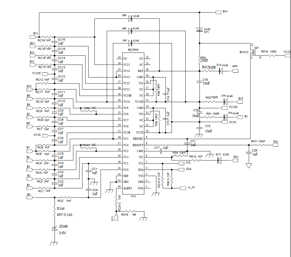
What is pin44/Alert for?  According to your reference schematic,  it is connected to MCU'S IO. Anything we need to do with it in the code?
#2
Per the literature, pin#6pin is on temperature detection. The schematic shows it is connected to  MCU through a diode isolation. Actually, it is found during debugging that the MCU must give a triggered high level before the IIC communicates normally. Would you please give reference code on this?
#3
About temperature detector of Pin13/TS2 and Pin18/TS3, if we don't use them, can we pull down the resistance to the ground? It is found that when the pull-down resistor is connected to the ground, the voltage read by IIC is all 0V.
#4
Most of the BQ76940 applications are on BMS, and there is no issue of power supply.  Our application is on a battery charger to manage the battery. We have the issue of power supply to BQ7640 itself: when the charger is not connected to the battery,  the chip is not powered at this time, IIC can not communicate. Our question is; can the BQ76940 be powered directly by the charger?
How do I connect? Can you give a reference circuit?
#5(see attached)
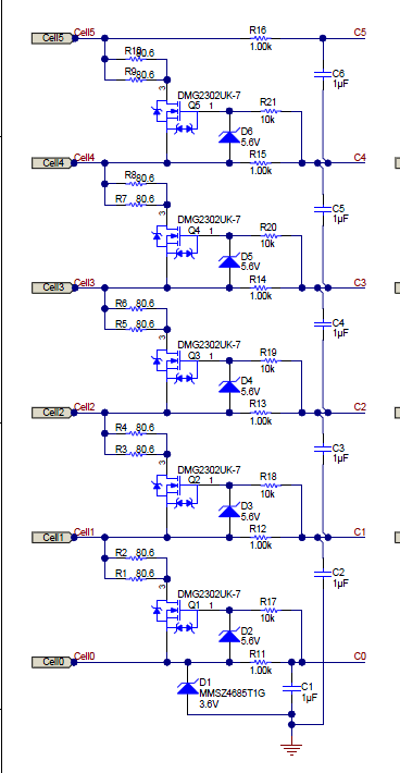
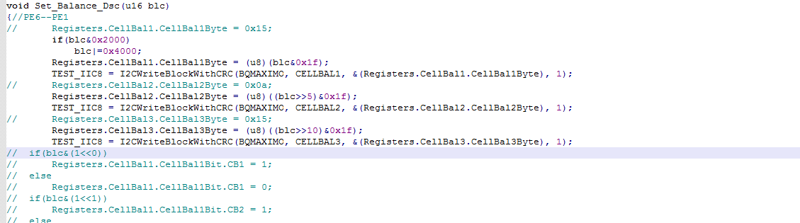
Regarding the cell balancing circuit, we need to increase the equalization current to 1.5A. Is it possible to directly change the resistance of the discharge resistors R1/R3/R5/R7/R9?  Do we need to handle this especially by code?
What is the trigger to balance: it is the voltage difference? What is the trigger to discharge for balancing?
  • Hi User,

    1. ALERT is to provide an interrupt to the MCU that something in the status register has been set.  It also has an input function to turn off FETs if it is not being driven high.  It should be cleared to avoid a supply offset current, see the electrical characteristics.

    2. Yes, the part must be "booted" with a rising edge on TS1 to wake up and communicate.  The data sheet shows the simple concept of a switch.  See the application note http://www.ti.com/lit/pdf/slua769 for alternatives, or some TI Designs. TIDA-00449 uses a MCU and has reference code but does not have the MCU powered separately and booting the device.  No reference code is known.

    3. If not used for temperature measurement the TSn pins should be connected to their local reference with a pull down resistor, 10k nominal in place of the thermistor.  Leaving the pins floating may prevent proper startup and result in XREADY fault.  Pulling TS2 and TS3 to VSS rather than the local reference will cause permanent XREADY as you have observed.

    4. The BQ76940 is intended to be used to monitor permanently attached cells.  Without cells you would need to keep the input voltages in acceptable range with a low enough impedance to allow operation.  You would also need to determine how to tell if the part were operating with a real battery or not.    The open circuit power is certainly one concern, another would be limiting transients as the battery is connected to the charging monitor.  While we thank you for your interest in the part we do not have a recommended circuit or method of connecting to the part.  I don't know if it would be suitable.

    5. Yes, balance current can be changed by changing the resistors.  Be sure to keep within the capacity of the FETs, and manage the heat which can result.   See http://www.ti.com/lit/an/slua749a/slua749a.pdf section 4 for a description of how the current is controlled.  Also the 1uF Cc capacitors C1, C2 etc give a long settling time during balancing so that voltage errors can be observed.  Newer reference designs use 0.22 uF or 0.1 uF caps.  The BQ76940 provides only the mechanism for balancing, it does not provide the algorithm.  The MCU will need to read the cell voltages under an appropriate condition and decide which cells are high, then duty cycle to bring them down to more closely match the lower voltage cells. You may find articles or videos on cell balancing helpful.

  • Hi Mastermind,

    I have further questions for your help:

    1 For discharging, the balancing circuit is using the resistor of 2.5R with the peak current of 1.7A and effective current of 1.2A.

       Is the 1uF capacitor the right choice for VC?

    2. As I mentioned before, we are using  BQ76940  on a battery charger instead of the popular application on BMS.  Regarding power supply to BQ7640 itself, can we power it by charger's circuit and the battery at the same time? Any risk of the design in this way? If it is the case:  when the charger started ready, IIC communication can be normal before the charger connects any battery?

    3. Per the cells connection table in the datasheet, SHORTING is implemented for different cells' configuration.  As our charger must stay ready for 12S, 13S, 14S Lipos at the same time, SHORTING is seemingly not feasible to our application. Is there any alternative way to configure cells dynamically by coding? Your suggestion will be highly appreciated!

    4 I am also attaching our charger's schematic. Your review and comment will be highly appreciated!! And we hope TI's 76940 blazes great for chargers!bq7694_2600_schemtic.pdf

  • Hi User,

    The expected use of the BQ76940 was for permanent attachment to cells, it is powered by and senses the cells, so there may be aspects of operating as a charger monitor which I do not understand.  

    1. The 1 uF Cc capacitors will slow the settling of the input filter and allow the bottom cell of each group to start measuring while the filter is still settling, see figures 5 and 6 of the application note http://www.ti.com/lit/an/slua775/slua775.pdf .  The smaller Cc capacitors would allow faster settling for better measurement.  With a charger the casual observer would not expect large transients on the cells which would need a heavy filter.

    2. The BQ76940 architecture has 3 cell groups, each with an abs max and which must have power to operate normally.  If powering the BQ76940 without cells attached the VC5X and VC10X will need some constraint so that the 60V shown does not distribute across the 3 cell groups in a manner to damage the IC.  Another challenge will be to avoid charging the battery unexpectedly through the BQ76940 circuit:  The BQ76940 must connect to the cells for sensing an power connection so that it can sense properly, if the BQ76940 also is connected to the charger circuit so that it is powered before the battery is attached, be sure to find a way to manage leakage from the BQ76940 circuit to battery.

    3. You could short at the cells when you connect to the 12, 13, or 14 cell battery leaving the connections at the IC pins open so that there are no parallel paths.  This is similar to the simple evaluation described with the EVM.  Notice that the top and bottom cells of each group must be used and 3 cells in each group should be used. 

    4. Schematic comments:

    The Cc size should be smaller with the 1k Rc filter resistors.  As noted next you might consider adjusting the Rc resistors with the power filter.

    The 10 uF Cf capacitors are needed for the architecture to keep the part operation out of VSHUT during short circuit timing since the power discharges through the input resistors as described in section 3 of the app note http://www.ti.com/lit/an/slua749a/slua749a.pdf.  Since you have a charger application and are not monitoring current, short circuit will not be a concern in your application. You will have the opportunity to select smaller Cf capacitors to better match the time constant of the monitor inputs. Do expect to provide some additional circuitry to avoid abs max violations before and during cell connection.  Consider figure 21 of the app note, you may still need some limit on these pins but the capacitor ratio between Cf and Cc may be better than 50:1 or 100:1 in the standard application. 

    RC38 and RC39 should not be installed if you are shorting at the cell terminals as noted earlier.

    REGOUT needs a capacitor at the pin even if you are not using it externally, the 1 uF min CL should be fine with no external usage.

    The BQ76940 architecture provides some challenges to a charger design, and is unfamiliar to us, so we may not have the best recommendations for your circuit. 

  • Hi, thanks for your helpful answers.

     After debugging on the physical PCBA, it is found: when CELL5 and CELL10 are being discharged, the voltage of CELL 6 and CELL 11 will be about 200 mv higher, respectively. All the other cells are running well with the correct voltage value!

     I am attaching the diagram: 1.PNG, and attaching the codes pertaining to discharging to balance: 2.PNG.

  • Hi User, 

    Three things look like they may contribute to the voltage situation.

    1. The diodes D73, D74, and D71 are not recommended and some users have reported damage in a traditional battery circuit.  These allow the supply pins to rise but not fall.  You are doing something special with the charger, but you don't want D69 conducting while measuring.  If you keep D71 you might add another series diode to D69.  The values of R01, R02, R03 are typically 1k.  

    2. The settling time of the 1k RC and 1uF CC can result in a voltage error during balancing particularly on cells 1, 6, and 11.  CC is often smaller to avoid this.

    3. The path resistance in B5, B10 is shared and during balancing can show a voltage in cell 6 when cell 5 is balancing and cell 11 when 10 is balancing as you report.  See http://www.ti.com/lit/an/slua749a/slua749a.pdf figure 8.  Usually the opposite is also occurs, perhaps the diodes in the power supply pins are causing that to be hidden.

    As mentioned before, you may need some method to keep then group power pins and cell sense pins within the abs max limits.

  • Thanks a lot, after trying fixing according to you clues, we are still stuck there.

    As there are three contiguous sets of 5 cells: Cells 1-5/Cells 6-10/ Cells 11-15, is the clock synchronized between the three sets? It is found that the voltage readings and driver discharging within the same set are synchronized.

    The clocking within the three sets is not synchronized.

    See the picture in detail: when cell 5 is discharging to balance, the sampled voltage will be pulled up (about 170-200 mv higher). It is also happening to CELL10/11.

    Please help! Thanks a lot!

  • Hi User,

    The sampling is not synchronized between the cell groups or sets.  They start approximately the same but can drift over time.  Within the group after the balancing time there is 1 rest interval before cells are measured sequentially, see http://www.ti.com/lit/pdf/slua775 for more information if interested. 

  • Hi Mastermind,

    We did look into all the cues you recommend. But still it happens: it is found: when CELL5 and CELL10 are being discharged, the voltage of CELL 6 and CELL 11 will be about 200 mv higher, respectively. All the other cells are running well with the correct voltage value!  

    We did also try to fix it by coding but we worry it is risky! Fixing on the circuit will be preferred!

    Thanks in advance!

  • Hi User,

    As mentioned above, D73, D74 are unusual and would seem a risk to normal operation. 

    Voltage increase of Cell 6 when Cell 5 is balancing is a common sign of common path resistance with the B5 net or portions of it pulling down from the balance current load.  You may need to measure to determine what is moving.  VC5X would not apparently move unless B5 moved, but if it did it could drop below B5 because of the diode mentioned and pull VC0 down also.  Again you will need to measure.  And the larger capacitor shown on the schematic (1uF) can hold a residual voltage, more  normally observed when a cell in the same group is balancing.