This thread has been locked.

If you have a related question, please click the "Ask a related question" button in the top right corner. The newly created question will be automatically linked to this question.

UCC28702: UCC28702

Part Number: UCC28702
Other Parts Discussed in Thread: UCC28700EVM-068

Hi,

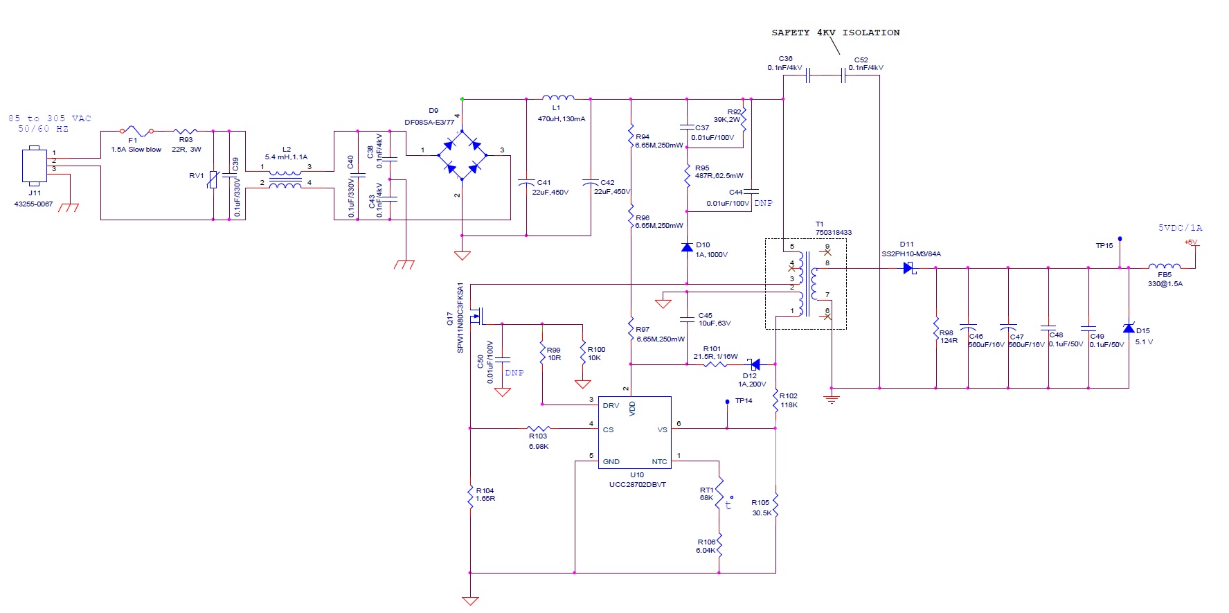
we are facing issue with UCC28702 design. Design is taken form WEBBENCH.

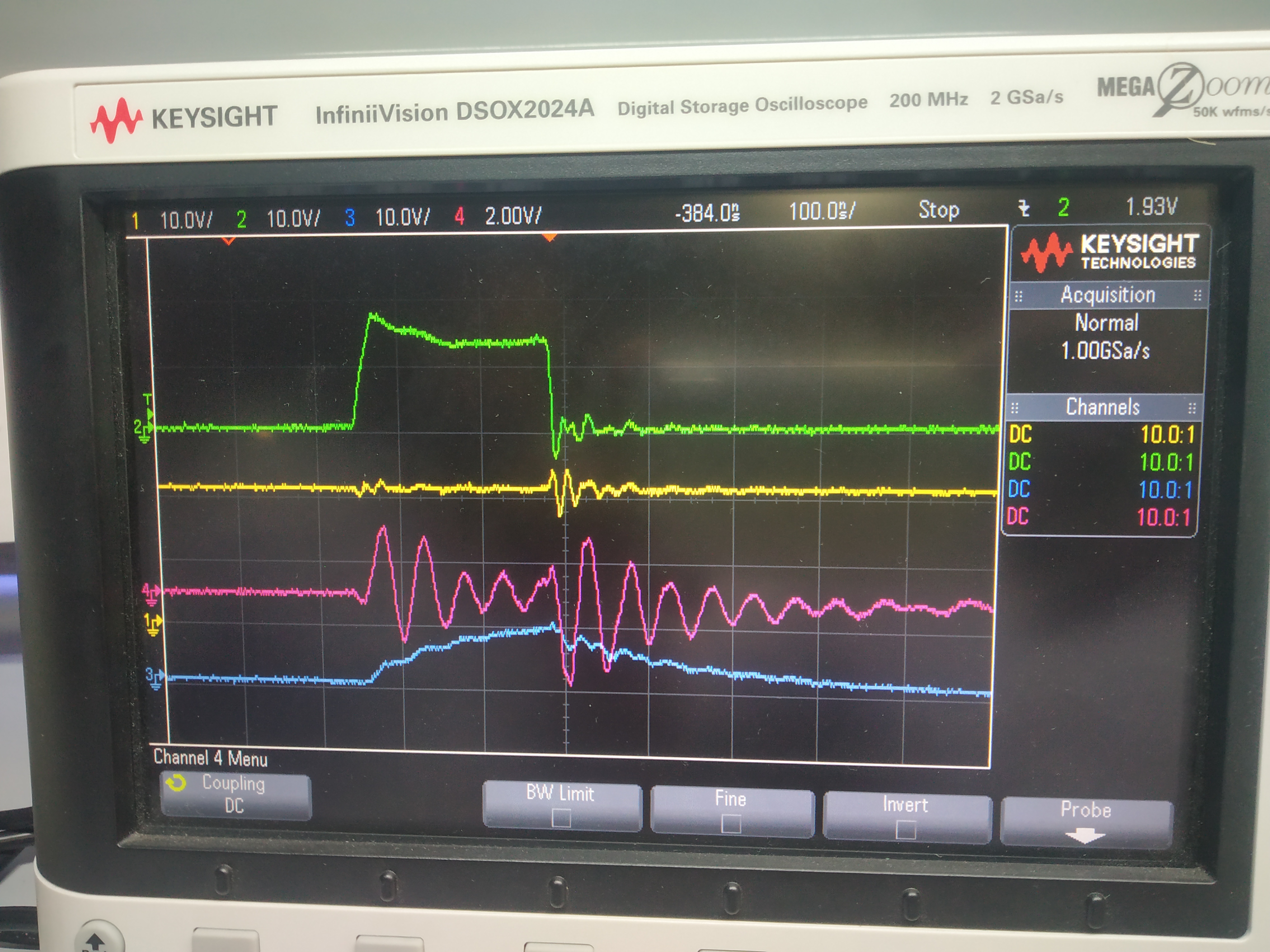
Unable to switching ON the power supply. the VDD pin of UC28702 is pulsating in between 21V to 8V.

Unable to getting the DRV pulse.

  • Hi

    First off I’d like to share the following debug app note we have for UCC28702 and the rest of our PSR flyback controllers http://www.ti.com/lit/an/slua783/slua783.pdf.  This document helps explain how to debug issues such as this.

    UCC28702 has several fault protections built into the device.  Details of all the various fault protections are in section 8.3.2 (page 12) of the UCC28702 datasheet.  When one of these fault conditions are triggered, UCC28702 will go into a UVLO restart.  This will cause the UVLO voltage to drop down to the VVDD(OFF) threshold before automatically restarting by charging VDD to VDD(ON).  If the fault condition has not been cleared by the time VDD(ON) is reached, UCC28702 will go into another fault shutdown cycle.  This is probably what is causing VDD to have a pulsating waveform.

    What we recommend you do is measure VDD, Vaux (not VS pin directly since it’s sensitive to parasitic capacitance), CS and DRV pins to see which fault is causing the shutdown.  After this we recommend you modify your design to prevent the fault shutdown from being triggered.  Since Webench is an ideal calculator there are some parts of a real circuit that it cannot simulate, such as parasitic capacitance and inductances from non-ideal components and PCB traces, which need to be accounted for in a design with bench debug. 

    Best Regards,

    Eric

  • Hi Eric,

    Thanks for the data and your support. Please find the attached waveform I found. Green one is gate drive, pink one is Auxiliary voltage and Blue one is pulse on CS pin. It seems detecting fault on CS pin.Please guide me   in this regard.

  • Hi

    The auxiliary waveform (pink) does not look correct.  It should look like Figure 13/14 (page 13/14) in the UCC28702 datasheet.  I recommend that you verify that your layout follows the recommendations in section 11.2 (page 25) of the UCC28702 datasheet.

    From your measurement it also shows that 10V is applied across CS pin.  This is well in excess of the 1.5V fault shutdown limit and the 5V abs max rating of this pin.  I recommend you verify that this pin is being measured correctly, and if so make sure it's not reaching the over current limit.

    Best Regards,

    Eric

  • Hi Eric,

    We verified layout and it seems OK. can you please confirm the circuit and transformer Design is OK?

  • Ram

    The connections on your schematic look correct.

    I recommend you use our design calculator http://www.ti.com/lit/zip/sluc381 

    Best Regards,

  • Hi Eric,

    Thanks for your support.

    I unable to open the file, due to I don't have  Mathcad tool. Can you please share the file in Excel format?

  • Ram

    Here is an excel version of the design calculator for UCC28702 http://www.ti.com/lit/zip/sluc408

    Best Regards,

    Eric

  • Hi Eric,

    Thanks for your support. verified the calculation as per your reference file.

    According to that modified the values and followed SLUA653C reference design and used 750312723 (wurth) transformer.

    But still we facing same issue. Can you please support in this regard.

    Thanks in advance.

    Ramgopal

  • Ramgopal

    Per my message on Sep 3, I recommend that you verify what the maximum voltage on the CS pin is.  Your waveform earlier shows 10V applied to the CS pin, which is well in excess of its 5V abs max rating.

    The auxiliary voltage you show is also not correct.  The aux winding needs to look like figure 13/14 of the UCC28702 datasheet.  First I recommend that you verify that you don't have any bandwidth filter or any other frequency limit on your sensing.  It's important that the transformer aux winding (pin 1-2), VS resistor dividers R102 and R105 along with the VS pin have a very small current loop area and small plane to minimize any parasitic capacitance and inductance.

    Best Regards,

    Eric

  • Hi Eric,

    Thanks for your reply support.

    We modified the our circuit as per the TI evaluation board (SLUA653C) and used recommended transformer 750312723).

    We got the output and the circuit function fine. It is working fine in input voltage range from 85-265VAC.

    Actually we need the design, it should work from 85-310VAC input range. Can you please suggest and need to consider changes in evaluation board schematic.

    And also suggest how to achieve EMI/EMC compliance. 

    Thanks in Advance.

    Ramgopal.

  • Ramgopal

     The transformer 750312723 is used on the EVM UCC28700EVM-068.  This design, including the transformer, is designed for an input of 90-265VAC.  

     In order to modify this design to work for a higher and wider voltage range you will need to modify the design.  You can use our excel design calculator http://www.ti.com/lit/zip/sluc408 to determine which component values need to change.  Please also note that the input voltage will be higher than the board is originally designed for, so we recommend that you verify the component voltage ratings and PCB spacing are adequate.

     Best Regards,

    Eric