This thread has been locked.

If you have a related question, please click the "Ask a related question" button in the top right corner. The newly created question will be automatically linked to this question.

TPS650864: Question of how to use

Part Number: TPS650864
Other Parts Discussed in Thread: TPS650861

Hi,

My customer chose TPS6508641.
1. BUCK1 becomes the external resistance setting, can it variable of output voltage by registers?
  Is there change voltage by only external registers?
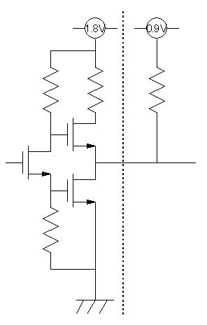
  Voutput = VFB_EXT_BUCK1 x (1+ Rup/Rdn)
  Is this calculating formula all right?

2.In the Figure 6-9., it use VTTLDO for MGTRAVCC, may we use VTTLDO for DDR and use LDOA3 for MGT?

Regards,
PAN-M

  • Hi PAN-M, 

    1. BUCK1 output voltage cannot be changed by I2C for TPS6508641. When the part is set to ext FB you can only change the output voltage by changing the resistor values. The equation above is correct in regards to Vout. We recommend using 294 kohm and 25.5 kohm resistors, giving a 5V output for BUCK1. 

    2. If you would like to change what the rails connect to we recommend using TPS650861, which is a user programmable version of TPS6508641.

    Best regards,

    Layne J

  • Thank you for answer.

    I think that our customer does not change the device.
    Do you not have any problem even if you use VTT LDO for DDR because Sink/Source capability have?

    Regards,
    PAN-M

  • Hi PAN-M,

    TPS650861 is a pin to pin exact replacement for TPS6508641, the only difference being TPS650861 is user programmable for their use case. VTT LDO will be 1/2 of the output voltage of BUCK6, which will be 0.9V for TPS6508641. This voltage is likely going to be too low to work with DDR. If there is a case where this voltage is usable for a specific output, it will function like a normal LDO if no feedback is provided.

    Best regards,

    Layne J

  • Let me confirm it.

    Both devices output to VTT with the voltage of VIN_VTT as 1/2.
    The voltage to input into VIN_VTT is the output of BUCK6.
    VTT becomes 0.9V because the default voltage of BUCK6 of TPS6508641 is 1.8V. 
    The default voltage of BUCK6 of  TPS650861 is 0V. 
    When I want to set VTT to 0.75V, 1.8V of the default of BUCK6 is too high. (VTTQ=1.5V)

    What is "programmable" what you say? BUCK6? One time memory?

    Best Regards,
    PAN-M

  • Hi PAN-M,

    TPS650861 is a blank device that allows the user to perform the one time programming on the device. The default voltage of BUCK6 on TPS650861 is set to 0V for a blank unit. The user can configure the buck controllers of this device (BUCK1/2/6) to have an output voltage between 0.41V and 3.575V during one time programming. This would allow them to configure the default output of BUCK6 for 1.5V or any other voltage they want in that range. The customer can use this programming capability to set each rail to their desired output voltages.

    Distributors Arrow and Avnet are also currently providing custom programming for these devices now.

    Best regards,

    Layne J

  • Could me ask you question one more?

    In Figure 6-9, what should the power device of VTT use?

    Regards,
    PAN-M

  • Hi PAN-M,

    VTT in Figure 6-9 is connected to VPS_MGTRAVCC, which is the PS-GTR Transceiver supply voltage for the Xilinx Zynq UltraScale+ ZU2CG ± ZU5EG2. This rail is expecting 0.85V to 0.9V. 

    Best regards,

    Layne J

  • My question is a question to say where VTT power of the DDR memory is supplied from.

    Figure 6-6 has it, but figure 6-9 does not have it.
    My customer thinks about a method to supply VTT power(0.75V) of the DDR.
    Is external VTT power supply necessary?

    Is the writing of TPS650861 of Disty free?

    Best Regards,
    PAN-M

  • Hi PAN-M, 

    I believe in that use case you would need to supply VTT externally. I will need to check with the expert who designed this block diagram and get back with you when I hear from them.

    Best regards,

    Layne J

  • Hi PAN-M,

    Figure 6-9 features DDR that does not require external termination. The DDR part number is MT53B256M32D1 and according to the datasheet has On Die Termination. If your customer wishes to use DDR that requires external termination they can use TPS650861 and program LDOA3 to provide the corresponding voltage. 

    Best regards,

    Layne J

  • Hi,

    Thank you for support and information.
    I think that LDOA3 does not have ability of the Sink/Source.

    When the port is low, the 0.9V power is source, and when the port is high, the 0.9V power needs sink ability.
    Therefore, the power supply of VTT thinks that VTT LDO or external power is necessary.


    The absolute rating of VDDQ was more than 1.9V when I watched a datasheet of DDR3.
    Therefore, I think that even start up of VDDQ of 1.8V may not have any problem.

    As a matter of course, the CPU cannot use the DDR until the CPU set the DDR voltage.

    Please teach me only sink/source ability of LDOA3.

    Regards,
    PAN-M

  • Hi PAN-M,

    I am looking into your question and will get back with you when I have an answer. 

    Best regards,

    Layne J

  • Hi PAN-M,

    LDOA3 does not have sink/source capabilities. If you need sink/source for your design use VTT_LDO and you can use LDOA3 to replace VTT_LDO for VPS_MGTRAVCC.

    Best regards,

    Layne J