This thread has been locked.

If you have a related question, please click the "Ask a related question" button in the top right corner. The newly created question will be automatically linked to this question.

UCC27712-Q1: Constant ON or Constant OFF Condition

Part Number: UCC27712-Q1
Other Parts Discussed in Thread: SN6501, UCC27712

Dear, Sir.

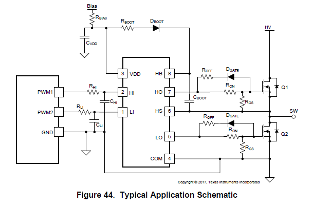
The datasheet describes the constant ON or constant OFF condition. It also

describes the boot-strap for VHB is hard to realize that.

1. Could you please let me know the bias structure for VDD, VHB?

   Sorry, I acn't find out that.

2. Nomrally, HI=High & LI=Low OR HI=Low & LI=High under such operation.

   Does it mean the interlock function automatically avoid both output being High

   even if HI=High & LI=High?

   If yes, How to determine which one should be ignored, output set Low?

I am hoping to get your advice.

Best Regards,

H. Sakai

  • Hello Sakai,

    Thank you for the interest in the UCC27712-Q1. Regarding the bias structure for VDD and VHB. The VDD provides the voltage for the internal IC blocks referenced to the COM pin, and the VHB-VHS provides the bias voltage for the HB IC blocks referenced to the HS pin. For providing the bias, VDD is supplied externally referenced to ground as with most IC devices. The HB-HS bias in most applications can be achieved with an external boot diode, and recommended resistance, connected to VDD and HB pins. The VHB bias is provided when HS switches close to ground and the VDD capacitor charges the HB capacitor thru the boot diode.

    Regarding the interlock. When both HI and LI are in the high state, both LO and HO are turned off to prevent MOSFET shoot thru. This state will remain as long as LI and HI are both high. When one of the inputs goes low, the other pin high input will result in the output returning to the high state.

    Confirm if this addresses your question, or you can post additional questions on this thread.

    Regards,

  • Dear, Richard-san. 

    Thank you so much for all of your teachings. 

    I suppose the normal boot-strap won't be operated under 100% duty especially 

    for high-side FET due to the limitation on Cboot charged energy. 

    I would like to know how to realize 100% duty operation for the high-side FET

    without the boot-strap. 

    Please give your advice. 

    Best Regards, 

    H. Sakai

  • Hello H. Sakai,

    For 100% duty cycle on the high side driver, a floating bias supply for HB-HS needs to be provided so that the high side bias will stay within the UVLO operating range with DC on the high side driver. TI has a small simple solution with the SN6501 transformer driver in a SOT23 package. below is a diagram of this circuit for the UCC27712 half bridge driver.

    The design details can be found in the SN6501 datasheet at

    http://www.ti.com/lit/ds/symlink/sn6501.pdf

    Confirm if this addresses your questions, or you can post additional questions on this thread.

    Regards,