This is the current schematic I use. I use TPS55340PWPR.
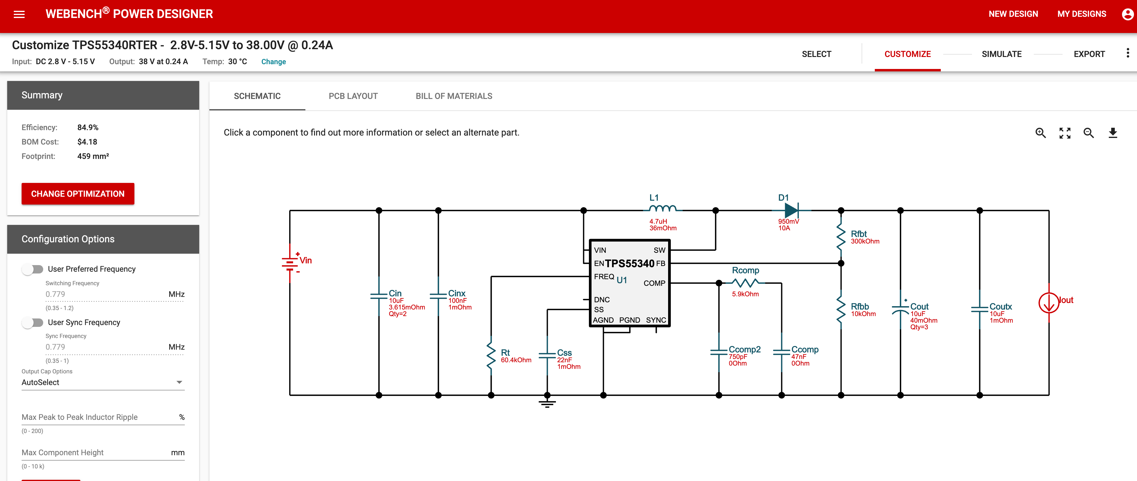
The WEBENCH recommended me to use B560C-13-F 60V Schottky diode and the 4.7uH XAL5030-472MEB inductor.
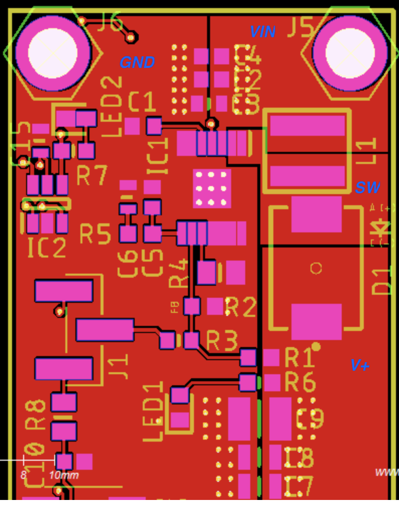
All the resistors have 0.1% tolerance with 1/8W Power rating and 0603 (16mm x 08mm) size.
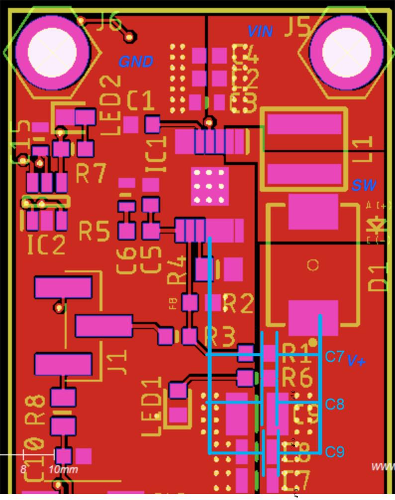
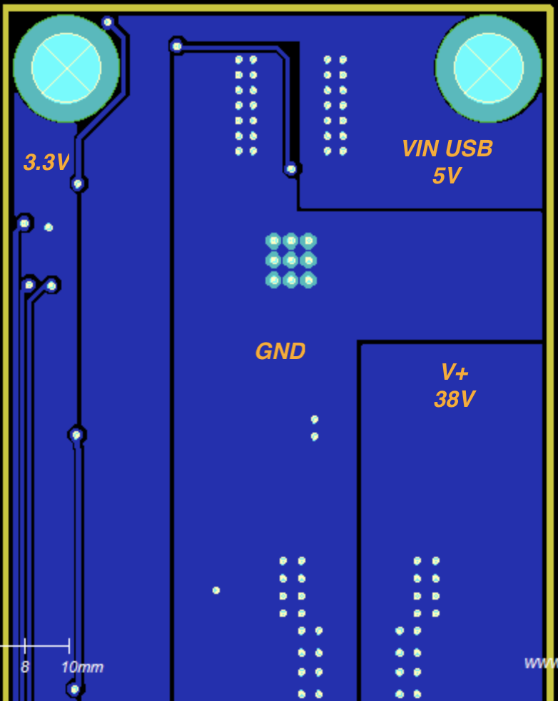
I removed the "thermal relief" (polygon trace) to swallow the GND pads. I placed
CIN: C2 10uF + C4 10uF + C3 15uF
COUT: C7 470nF + C8 470nF + C9 10uF
with vias.
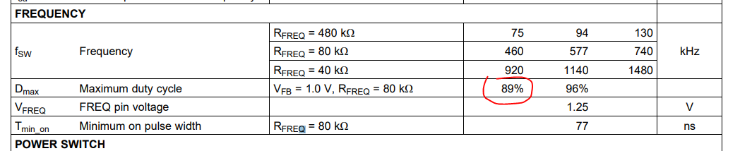
R1, R2, R3 is used for the feedback loop and I referred PMP15037 (DAC signal to decrease VOUT)
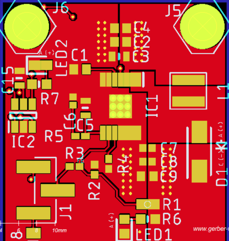
Top (FR-4, 1.6mm thick 2 layered PCB)
Bottom
Does the layout look fine? Do I need more vias?