This thread has been locked.

If you have a related question, please click the "Ask a related question" button in the top right corner. The newly created question will be automatically linked to this question.

TPS40305: TPS40305 Ripples Issue

Part Number: TPS40305

Hi,

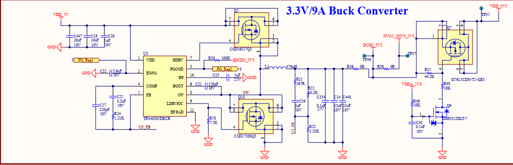
I am using TPS40305DRCR switcher IC to generate 3.3V from 5V input. It is designed to generate 3.3V with 9A load. The switching frequency is 1.2 MHz. When I connect an external load of 1A or more, I am receiving ripples at input of the switcher at 1.2 MHz frequency and as I increase the load, the ripples' amplitude increases and ripples at same frequency are received at output side. Can you please tell me why the ripples are reflected back on input at switcher's frequency? Please provide the solution and root cause for this problem.

I have attached schematic snapshot and waveform for your reference.

Thanks in advance!

Sahil Nayak

  • Hi TI Team,

    Any update on this?

    This is a very critical issue for us. Please suggest the solution ASAP.

    Awaiting for your quick response.

  • Sahil,

    I will get someone to look at it.  But I can tell you up front that this is normal.  The AC circulating current flows through the input capacitors and will cause the ripple you observe.  If it is too much, you can increase the input capacitance and add some additional HF bypass capacitance such as 0.1 uF, 0.01 uF, 0.001 uF etc.

  • Sahil Nayak,

    As John Tucker mentions, this is normal for a BUCK switcher.

    A BUCK switcher operates by drawing  discontinuous current from the input and sourcing continuous current at the output in order to efficiently convert a high input voltage to a low output voltage.  With each "On-time" pulse the high-side FET (Q5 in your schematic) turns on and the inductor draws the full output current from the input capacitors, discharging the input capacitors.  During each "Off-time" the low-side FET (Q18 in your schematic) turns on and the inductor draws the full output current from ground.

    In this way, the average input current is approximately IOUT x Duty Cycle [ On-time / (On-time + Off-time) ], and the Input power is similar to the total output power (VOUT x IOUT)

    For 5V to 3.3V @ 1.2Mhz, the On-time is approximately 3.3V / 5V  * 1/1.2MHz = 550ns.

    Under 9A of load current, that will draw 4.95uC of charge from the input capacitors.

    With 21uF of input capacitance, we would expect at least 250mV of input ripple at the input.  Likely more due to DC bias effect of a 5V AC bias on a 10V rated input capacitors and the ESR and ESL of the input capacitors reducing their effective capacitance at 1.2MHz and above.

    In order to reduce the input ripple you can:

    1) Reduce the dynamic impedance of your source at a frequency of 1.2MHz so that the sourcing supply can provide some dynamic current during the switching cycles.  This could prove extremely difficulty with a lab-supply that has long wires adding significant inductance, but could be more practical in an integrated solution where the 5V sourcing supply and the TPS40305 based 5V to 3.3V converter are on the same PCB.

    2) Increase the voltage rating of the Input Capacitors.  Because capacitors lose capacitance as their DC voltage increases, it is likely that the input voltage ripple will be lower if you use 16V or 25V rated 10uF input capacitors instead of 10V rated input capacitors.

    3) Increase the input capacitance by changing the 10uF input capacitors to higher values, such as 22uF capacitors or adding additional input capacitors.  As noted above, the input ripple is inversely proportional to the Input Capacitance.

    Note:  Due to the high switching frequency, it is unlikely that adding Electroytic or Polymer capacitors to the input will have much impact on the input ripple voltage, as those capacitors will be entirely dominated by ESR at 1.2MHz.

    4) To reduce the high-frequency spikes that appear on the 5V supply with each switch, you will need to add high-frequency bypass capacitance from 5V to ground.  These are generally smaller, lower capacitance capacitors placed very close to the drain of Q5 and source of Q18)   Adding capacitance less than 1.0uF (2.2 to 100nF) close to the switching FETs would prevent those high megahertz switch ringing from propagating along the 5V supply.

    5) While it will not reduce the VIN ripple seen by the TPS40305, converter, adding a ferrite bead between the 5V sourcing supply and the bypass capacitors will contain the 1.2MHz switching noise to the converter and prevent it from propagating to other devices on the 5V sourcing supply.