This thread has been locked.

If you have a related question, please click the "Ask a related question" button in the top right corner. The newly created question will be automatically linked to this question.

BQ79606A-Q1: How to perform Open-wire detection

Part Number: BQ79606A-Q1

Hi,

I have four questions about BQ79606:

1.As the datasheet describes BQ79606 can pull down VC1-VC6/CB1-CB6 and pull up VC0/CB0 then read ADC value to do the open-wire detection. But could you tell me what exactly the ADC value difference will be between the normal connection case and open-wire case and why?

2.Why the VC0 and CB0 have to be pulled up rather than pulled down?

3."9.2.1.2.6 CB Input" section says "If a connection to cell1 negative terminal is open the IC bias current will flow through the CB1/VC1 pins and then to the cell2 negative module terminal, causing CB1 and VC1 pins to go below the minimum voltage recommended with respect to pin AVSS", where does this IC bias current comes from?

4.In the design recommendation, it says VC series resistance should be 4 times of CB resistance for the best hot-plug performance. Why this 4 times resistance setup can give me the best hot-plug performance? 

Thank you for your reply!

  • Hi Taoran,

    Have you taken a look at our safety manual? It is online here:http://www.ti.com/lit/an/slua822c/slua822c.pdf and should answer many of your questions about the flow. The change in ADC readings will depend on how much time you are waiting between reads and you will just need to calculate this based on Cdv/dt. VC0/CB0 are current source rather than sink so this does not pull to below AVSS. The IC bias current is current consumed by the device channels for the measurement (the spec is in the EC table for bias current). The 4 times CB resistance ratio is important for the VC/CB short check diagnostic so that the voltage drop is more pronounced when doing the comparison.

    Regards,

    Taylor

  • Hi Taylor,

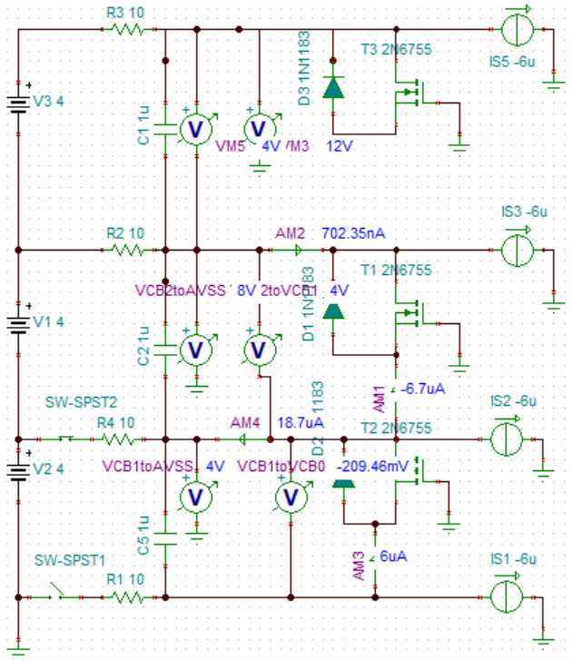
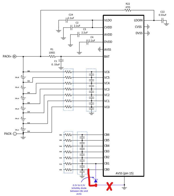
    I try to simulate the CB circuit in the TINA, and find out it's the differential voltage between the CB1 and CB0 may be pulled below the -0.3V and violates the specs, rather than the voltage of CB1 to AVSS, which is different from the datasheet. Is there something wrong with my simulation?

  • Hi Taoran,,

    There is a cap from VC0 to GND and you need to source the current not sink.

    So, you are going to charge up the cap on VCO to GND. So VCO voltage will increase.

    add a cap on VCO to gnd and source the current not sink on VCO.

    Update this and run TINA again.

    Roger

  • Roger,

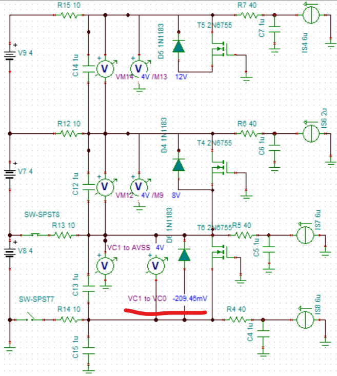
    Thank you for your response, but still, it's the differential voltage between VC1 and VC0 go below the ground. Sorry, I really want to figure out this problem.

    It makes sense that charging the cap between the VC0 to GND, and the VC0 voltage increases. And because of the balancing MOSFET body diode, the VC0 will increase to the (VC1+VforwardBD), causing the differential voltage between VC1 and VC0 go below the ground. 

    So I suppose the schottky diode should be added between CB1 and CB0 rather than between the CB1 and GND, is that right? The following is the modified TINA circuit, and the solution to solve this CB0 floating problem.

    Thanks again.


  • Hi Taoran,

    The simulation is still incorrect as only the VC0 line is a current source. All other VC pins are current sinks.

    Regards,

    Taylor

  • Hi Taoran,

    I am going to close this tread for now.

    Let us know if you still having an issue.

    As Taylor said, VCO is sourcing not sinking.

    Roger