This thread has been locked.

If you have a related question, please click the "Ask a related question" button in the top right corner. The newly created question will be automatically linked to this question.

LP55231: LEDs driver does not Turn ON LED lights

Part Number: LP55231

Dear support,

If this is not the right support page, please refer me to the correct page for the LP55231 LED Driver (9 Channel RGB / White LED Driver with Internal Program Memory and Integrated Charge Pump - WQFN)

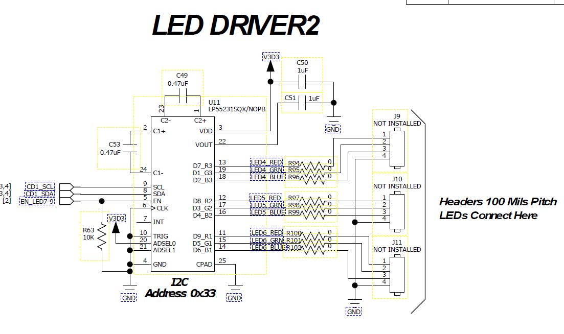
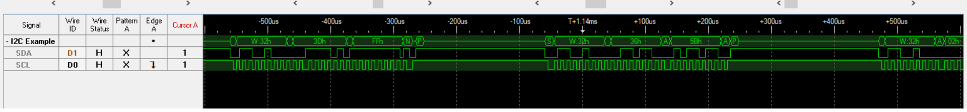
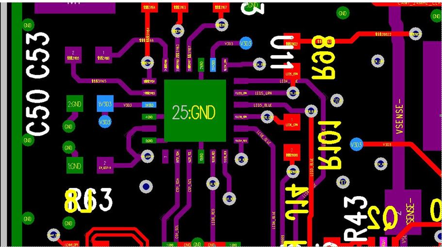
I am writing I2C commands to the device, and I see the commands go out, but the LEDs RGB connected to J5 in my schematic below never turn on.  I have the trigger button grounded, and in the datasheet it said if not used, ground it.  So I grounded it.

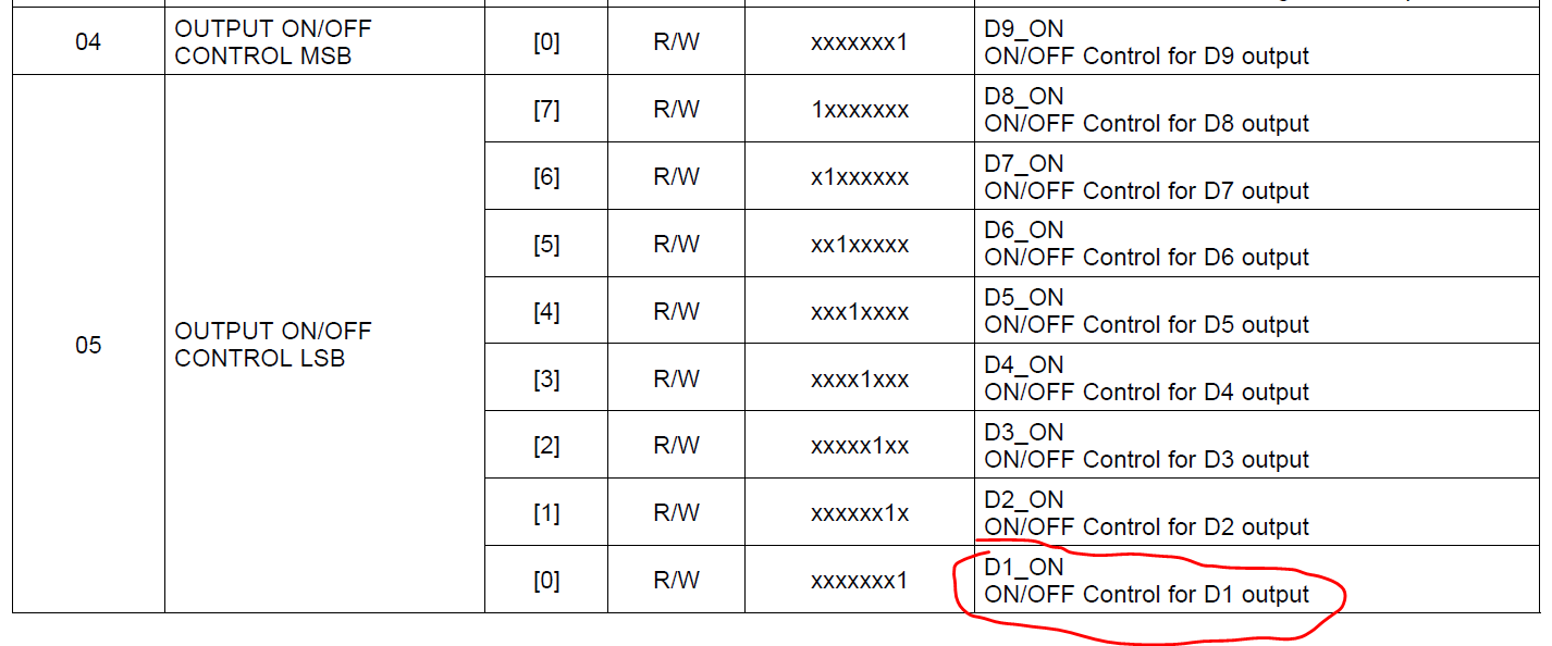
I am having difficulties understanding how to just turn it ON.  I have written the current register to 17.5mA, I have written the register for the LED, and you would think it would turn on, but it is like the ON command is missing.  Are there any app notes on how to simply turn ON one led?

I want to know if the hardware is OK, and out of 20 boards, none work, we have checked the layout, and the schematic, and all seems in order yet, it refuses to turn ON the LEDs.  Please advise what is the proper way to write to this device.

Kindly,

Robert

  • Hi Robert,

    Could you help to re-post your schematic? It seems died in original thread.

    And how you sent I2C commands, GUI or MCU simulation?

  • I don't know how to attach the image in this forum. I pasted it in the text area. If you send me an email, I can reply with the schematic section.

  • I have a microcontroller  i2c bus connected to the chip. I wrote c code to communicate with it.

    RR

  • Dear Hardy,

    The schematic I sent is for 2 LED drivers.  I have written C-code in a microcontroller to send command via I2C bus to the device.  I have a logic analyzer hooked on the bus monitoring the MCU to ensure the command reach the IC on its bus.  the image attached shows an example capture for some commands I sent.

    Here is some "experimental" code I wrote trying multiple things... the code is raw and I have not cleaned up comments, and I am using repetition command rather than doing it properly in the interest of saving time.  I need to understand few things.

    1. In the hardware the TRIG pin is hard wired to GROUND.  Is this a problem?

    2. The INT pin is floating is this a problem?

    3. What should be the proper sequence to turn on the LEDs?  All I want to do is just turn on a RED, GREEN, and BLUE LED connected to my custom hardware.   It would be nice to just have a pseudo code that show how to turn on LEDs without the intricate programs one can do on this chip.  I just want to Turn On, the red, then the green, then the blue.  That is all.  I am just trying to prove the hardware is good, and that the MFG house assembled the chip correctly.

    -  I have tried to setup the current, the PWM register, I have initialized several register, and I can see the MCU writing correctly, but the chip is simply unresponsive.

    - Visual inspection on the board shows the chips is soldered down correctly, yet no light comes ON.

    From my perspective, the LAYOUT is in order, the schematic fairs good with sparkfun breakout board using the LP55231, the only difference between this board and mine is the TRIG pin (which I am not using) being grounded, and INT pin floating.

    We are at a loss as to why it refuses to work.  All 25 board are like this, and I refuse to believe the assembly temperature killed all the chips, or that everyone of those chips have cold solders.  It is more likely the code is sending the correct sequence to this part.  This is where I need your assistance.

    Best,

    RR

    #include "CCSUSB.h"
    #include <usb_cdc.h>
    
    /*
    Initialize MCU I2C1 SSP ENGINE
    The PIC24FJ256GB206 has its SDA1, SCL1 on
    SCL1 = TQFP-64 PIN 44, and demo board maps to D10 header PIN 20
    SDA1 = TQFP-64 PIN 43, and demo board maps to D9 header PIN 21
    Ground is on header pin 33 and 34
    */
    #use i2c(MASTER, SCL=PIN_D10, SDA=PIN_D9, SLOW, FORCE_HW, STREAM=I2CM1) 
    
    /*
    Use the LCD - Define the connections on the hardware
    */
    #define LCD_ENABLE_PIN  PIN_D0                                    
    #define LCD_RS_PIN      PIN_D1                                    
    #define LCD_RW_PIN      PIN_D2                                    
    #define LCD_DATA4       PIN_E6                                    
    #define LCD_DATA5       PIN_E7                                  
    #define LCD_DATA6       PIN_D6                                    
    #define LCD_DATA7       PIN_D7                                    
    #include <lcd.c>
    #define LP55321_EN      PIN_B13
    #define LP55321_I2C_WADDR    0x64        //Write
    #define LP55321_I2C_RADDR    0x65        //Read
    
    //32 entries program
    static const unsigned long program[] = {
        0x9c10,        //0 map start
        0x9c9f,        //1 map end
        0x66ff,        //2 ramp up
        0x0200,        //3 wait
        0x07ff,        //4 ramp down
        0x9d80, // 5 map next
        0xa002, // 6 loop to 2
        0x000a, // 7 - empty placeholder
        0x0005, // 8 - empty placeholder
        0x000a, // 9 - empty placeholder
        0x0005, // a - empty placeholder
        0x000a, // b - empty placeholder
        0x0005, // c - empty placeholder
        0x000a, // d - empty placeholder
        0x0005, // e - empty placeholder
        0x000a, // f - empty placeholder
        0x0001, // 10 map begin - start of 2nd page
        0x0002, // 11
        0x0040, // 12
        0x0004, // 13
        0x0008, // 14
        0x0080, // 15
        0x0010, // 16
        0x0020, // 17
        0x0100, // 18
        0x0020, // 19
        0x0010, // 1a
        0x0080, // 1b
        0x0008, // 1c
        0x0004, // 1d
        0x0040, // 1e
        0x0002, // 1f  map end
    };
    
    // register stuff
    static const unsigned char REG_CNTRL1 = 0x00;
    static const unsigned char REG_CNTRL2 = 0x01;
    static const unsigned char REG_RATIO_MSB = 0x02;
    static const unsigned char REG_RATIO_LSB = 0x03;
    static const unsigned char REG_OUTPUT_ONOFF_MSB = 0x04;
    static const unsigned char REG_OUTPUT_ONOFF_LSB = 0x05;
    
    // Per LED control channels - fader channel assig, log dimming enable, temperature compensation
    static const unsigned char REG_D1_CTRL = 0x06;
    static const unsigned char REG_D2_CTRL = 0x07;
    static const unsigned char REG_D3_CTRL = 0x08;
    static const unsigned char REG_D4_CTRL = 0x09;
    static const unsigned char REG_D5_CTRL = 0x0a;
    static const unsigned char REG_D6_CTRL = 0x0b;
    static const unsigned char REG_D7_CTRL = 0x0c;
    static const unsigned char REG_D8_CTRL = 0x0d;
    static const unsigned char REG_D9_CTRL = 0x0e;
    
    // Direct PWM control registers
    static const unsigned char REG_D1_PWM  = 0x16;
    static const unsigned char REG_D2_PWM  = 0x17;
    static const unsigned char REG_D3_PWM  = 0x18;
    static const unsigned char REG_D4_PWM  = 0x19;
    static const unsigned char REG_D5_PWM  = 0x1a;
    static const unsigned char REG_D6_PWM  = 0x1b;
    static const unsigned char REG_D7_PWM  = 0x1c;
    static const unsigned char REG_D8_PWM  = 0x1d;
    static const unsigned char REG_D9_PWM  = 0x1e;
    
    // Drive current registers
    static const unsigned char REG_D1_I_CTL = 0x26;
    static const unsigned char REG_D2_I_CTL  = 0x27;
    static const unsigned char REG_D3_I_CTL  = 0x28;
    static const unsigned char REG_D4_I_CTL  = 0x29;
    static const unsigned char REG_D5_I_CTL  = 0x2a;
    static const unsigned char REG_D6_I_CTL  = 0x2b;
    static const unsigned char REG_D7_I_CTL  = 0x2c;
    static const unsigned char REG_D8_I_CTL  = 0x2d;
    static const unsigned char REG_D9_I_CTL  = 0x2e;
    
    static const unsigned char REG_MISC     = 0x36;
    static const unsigned char REG_PC1 = 0x37;
    static const unsigned char REG_PC2 = 0x38;
    static const unsigned char REG_PC3 = 0x39;
    static const unsigned char REG_STATUS_IRQ = 0x3A;
    static const unsigned char REG_RESET      = 0x3D;
    
    static const unsigned char REG_PROG1_START = 0x4C;
    static const unsigned char REG_PROG2_START = 0x4D;
    static const unsigned char REG_PROG3_START = 0x4E;
    static const unsigned char REG_PROG_PAGE_SEL = 0x4f;
    
    // Memory is more confusing - there are 4 pages, sel by addr 4f
    static const unsigned char REG_PROG_MEM_BASE = 0x50;
    //static const unsigned char REG_PROG_MEM_SIZE = 0x;//
    static const unsigned char REG_PROG_MEM_END  = 0x6f;
    
    static const unsigned char REG_ENG1_MAP_MSB = 0x70;
    static const unsigned char REG_ENG1_MAP_LSB = 0x71;
    static const unsigned char REG_ENG2_MAP_MSB = 0x72;
    static const unsigned char REG_ENG2_MAP_LSB = 0x73;
    static const unsigned char REG_ENG3_MAP_MSB = 0x74;
    static const unsigned char REG_ENG3_MAP_LSB = 0x75;


    void main(void)
    {
       char c;
       unsigned int8 delay=0;
       unsigned char val = 0;
       unsigned char i = 0;
       
       LED_ON(GREEN_LED);
    //!   LED_OFF(YELLOW_LED);
    //!   LED_OFF(RED_LED);
    //!   
    //!   setup_adc(ADC_CLOCK_INTERNAL | ADC_TAD_MUL_2);
    //!   setup_adc_ports(MY_ANALOG_PORTS);
    //!   set_adc_channel(AN_POT);
       
       usb_init();
       
       lcd_init();
       delay_ms(1000);
       //printf(lcd_putc,"\a");
       printf(lcd_putc,"\aReady...");
       
       while (TRUE)
       {
          if (usb_enumerated () )
          {
             delay_ms(1000);
             LED_ON(YELLOW_LED);
    
             If (usb_cdc_kbhit () )
             {
                c = usb_cdc_getc();
    
                switch(c)
                {
                    case 'i':                       //Initialize the led driver
                    case 'I':
                    {
                        printf(usb_cdc_putc,"In Init\r\n");
                        printf(lcd_putc,"\a");
                        
                        output_low(LP55321_EN);
                        LED_OFF(RED_LED);
                        printf(lcd_putc,"INIT: EN = 0\n");
                        
                        delay_ms(500);
                        
                        output_high(LP55321_EN);
                        LED_ON(RED_LED);
                        printf(lcd_putc,"INIT: EN = 1");
                        
                        //writeReg(0x00 , 0x40);
                        i2c_start(I2CM1);                               //(S) Start Condition
                        i2c_write(I2CM1,LP55321_I2C_WADDR);             //(W) Write the Slave Address
                        i2c_write(I2CM1,REG_CNTRL1);                    //Send Command for REG D8 RED
                        i2c_write(I2CM1,0x00);                          //Logarithmic dimming control for D8 output
                        i2c_stop(I2CM1);    
                        
                        //writeReg(0x36 , 0x53);
                        i2c_start(I2CM1);                               //(S) Start Condition
                        i2c_write(I2CM1,LP55321_I2C_WADDR);             //(W) Write the Slave Address
                        i2c_write(I2CM1,REG_MISC);                    //Send Command for REG D8 RED
                        i2c_write(I2CM1,0x53);                          //Logarithmic dimming control for D8 output
                        i2c_stop(I2CM1);    
            
                        //Set drive current 
                        for(i = 0; i < 9; i++)
                        {
                            //writeReg(0x0n, value); set current
                            i2c_start(I2CM1);                               //(S) Start Condition
                            i2c_write(I2CM1,LP55321_I2C_WADDR);             //(W) Write the Slave Address
                            i2c_write(I2CM1,(REG_D1_I_CTL+i));               //Send Command for REG D8 RED
                            i2c_write(I2CM1,0xAF);                          //Logarithmic dimming control for D8 output
                            i2c_stop(I2CM1);                                 //(P) Stop Condition
                            
                            //writeReg(0x1n, value); set PWM
                            i2c_start(I2CM1);                               //(S) Start Condition
                            i2c_write(I2CM1,LP55321_I2C_WADDR);             //(W) Write the Slave Address
                            i2c_write(I2CM1,(REG_D1_PWM +i));               //PWM val
                            i2c_write(I2CM1,0xFF);                          //Logarithmic dimming control for D8 output
                            i2c_stop(I2CM1);                                 //(P) Stop Condition
                                                         
                        }
                            //Presumably this is to control the ON/OFF for the
                            //driver output... I am turning 0-8 D1-D8 ON
                            i2c_start(I2CM1);                               //(S) Start Condition
                            i2c_write(I2CM1,LP55321_I2C_WADDR);             //(W) Write the Slave Address
                            i2c_write(I2CM1,REG_OUTPUT_ONOFF_LSB);          //Set to log brightness
                            i2c_write(I2CM1,0xFF);                          //
                            i2c_stop(I2CM1); 
                            
                            //Turning ON the last BIT ON D9
                            i2c_start(I2CM1);                               //(S) Start Condition
                            i2c_write(I2CM1,LP55321_I2C_WADDR);             //(W) Write the Slave Address
                            i2c_write(I2CM1,REG_OUTPUT_ONOFF_MSB);          //Set to log brightness
                            i2c_write(I2CM1,0x01);                          //
                            i2c_stop(I2CM1);                                //(P) Stop Condition
                            
       
                        break;
                    }
                    
                    case 'a':                       //Start LED
                    case 'A':
                    {
                        
                        break;
                    }
                    
                    case 'f':
                    case 'F':
                    {
                        break;
                    }
                    
                    default:
                    {
                    
                    }
                }
                
             }
    //!         delay_ms(1000);
    //!         output_high(LP55321_EN);
    //!         LED_ON(RED_LED);
    //!         delay_ms(1000);
    //!         output_low(LP55321_EN);
    //!         LED_OFF(RED_LED);
          }
       }
    }

    CHIP LAYOUT ON CUSTOM BOARD

    Not all layers are turned on, the ground planes, etc..  Only top layer (purple), bottom layer (RED)  The charge pump caps are in the opposite layer through vias.  Is this an issue?  Vias can handle up to 1Amp.  I imagine the switching frequency is less than 20MHz.

  • Hi Roberto,

    Your schematic and layout is OK. And it is also no problem to ground the TRIG pin and float the INT pin.

    Maybe there are some issues with power up sequence. Could you help to check your code is following as below? To light up the LED, CHIP_EN bit should be written high and EN pin should be turn high.

    The Start-up delay is 500 μs. Then set charge pump mode to 1x or 1.5x.

    After that, turn on the LED channel you want.

    Finally adjust the PWM and current bit to light up the LED.

  • Dear Hardy,

    I will try that and get back to you.  It is possible that all these addresses are not receiving the correct value.

    So here is what I plan to sequence

    Register -> Value

    0x00 -> 0x40 (0100 0000) LP55321 Enabled

    0x36 -> 0x18 -> for automatic control  I guess I will try 0x08 (for to bypass mode), 0x10 (x1.5 mode), and 0x18 for automatic mode

    0x05 -> 0xFF ->  I want them all ON D1 - D8

    0x04 -> 0x01-> D9

    I will post back to if the results are positive.

  • I tried all that and didn't work.  I suspect the chips are bad.  What could cause them to be bad?

    RR

  • Hi Roberto,

    Can you read these registers after you write in?

    Do you have our EVM board? To confirm whether the chip is damaged, you could de-mount it from your board and solder it to EVM to test the function.

  • I do not have the demo board, but I have been focused on writing to the registers. I will try reading all the registers and see if I can.  What are the defaults so I can compare?

    Regards,

    RR

  • The datasheet shows table 3 with defaults but somebits are don't care. I suppose i will mask the don't care bits and compare.

  • Dear Hardy,

    I read the register and initially they read  0xFF, then I write only the register you highlighted, then I read back and the LED turn ON.  For some reason, if I don't read them first, writing to them won't work.  So I have to read them, then write them.

    For example I was turning on the RED.  Then I changed the code to turn on the Green.  The change won't take effect until I read all register, then write them.  This is bizzare why this is.  I was thinking the I2C bus capacitance was higher, and maybe the reading process charges the I2C lines, then writing them works.  So I changed the pull-ups from 4.99k to 2.47k and still the same thing.  It is not the pull-ups.  I put the scope the signals look good with a fast rising edge in both pull-up values.

    Why do I need to read them all and write them to make it work is a mystery.  I can't figure that out..

    READING REGISTERS....
    0 -> LP55231_REG_00 = 0x40
    1 -> LP55231_REG_01 = 0x00
    2 -> LP55231_REG_02 = 0x00
    3 -> LP55231_REG_03 = 0x00
    4 -> LP55231_REG_04 = 0x01
    5 -> LP55231_REG_05 = 0xFF
    6 -> LP55231_REG_06 = 0x00
    7 -> LP55231_REG_07 = 0x00
    8 -> LP55231_REG_08 = 0x00
    9 -> LP55231_REG_09 = 0x00
    10 -> LP55231_REG_0A = 0x00
    11 -> LP55231_REG_0B = 0x00
    12 -> LP55231_REG_0C = 0x00
    13 -> LP55231_REG_0D = 0x00
    14 -> LP55231_REG_0E = 0x00
    16 -> LP55231_REG_10 = 0x00
    17 -> LP55231_REG_11 = 0x00
    18 -> LP55231_REG_12 = 0x00
    19 -> LP55231_REG_13 = 0x00
    20 -> LP55231_REG_14 = 0x00
    21 -> LP55231_REG_15 = 0x00
    22 -> LP55231_REG_16 = 0x00
    23 -> LP55231_REG_17 = 0x00
    24 -> LP55231_REG_18 = 0x20
    25 -> LP55231_REG_19 = 0x00
    26 -> LP55231_REG_1A = 0x00
    27 -> LP55231_REG_1B = 0x00
    28 -> LP55231_REG_1C = 0x00
    29 -> LP55231_REG_1D = 0x00
    30 -> LP55231_REG_1E = 0x00
    26 -> LP55231_REG_1A = 0x00
    27 -> LP55231_REG_1B = 0x00
    28 -> LP55231_REG_1C = 0x00
    29 -> LP55231_REG_1D = 0x00
    30 -> LP55231_REG_1E = 0x00
    31 -> LP55231_REG_1F = 0x00
    32 -> LP55231_REG_20 = 0x00
    33 -> LP55231_REG_21 = 0x00
    34 -> LP55231_REG_22 = 0x00
    35 -> LP55231_REG_23 = 0x00
    36 -> LP55231_REG_24 = 0x00
    37 -> LP55231_REG_25 = 0x00
    38 -> LP55231_REG_26 = 0xAF
    39 -> LP55231_REG_27 = 0xAF
    40 -> LP55231_REG_28 = 0xAF
    41 -> LP55231_REG_29 = 0xAF
    42 -> LP55231_REG_2A = 0xAF
    43 -> LP55231_REG_2B = 0xAF
    44 -> LP55231_REG_2C = 0xAF
    45 -> LP55231_REG_2D = 0xAF
    46 -> LP55231_REG_2E = 0xAF
    47 -> LP55231_REG_2F = 0x00
    48 -> LP55231_REG_30 = 0x00
    49 -> LP55231_REG_31 = 0x00
    50 -> LP55231_REG_32 = 0x00
    51 -> LP55231_REG_33 = 0x00
    52 -> LP55231_REG_34 = 0x00
    53 -> LP55231_REG_35 = 0x00
    54 -> LP55231_REG_36 = 0x10
    55 -> LP55231_REG_37 = 0x00
    56 -> LP55231_REG_38 = 0x00
    57 -> LP55231_REG_39 = 0x00
    58 -> LP55231_REG_3A = 0x48
    59 -> LP55231_REG_3B = 0x00
    60 -> LP55231_REG_3C = 0x00
    61 -> LP55231_REG_3D = 0x00
    62 -> LP55231_REG_3E = 0x00
    63 -> LP55231_REG_3F = 0x19
    64 -> LP55231_REG_40 = 0x00
    65 -> LP55231_REG_41 = 0x00
    66 -> LP55231_REG_42 = 0x00
    67 -> LP55231_REG_43 = 0x03
    68 -> LP55231_REG_44 = 0x48
    69 -> LP55231_REG_45 = 0x00
    70 -> LP55231_REG_46 = 0x00
    71 -> LP55231_REG_47 = 0x00
    72 -> LP55231_REG_48 = 0x00
    73 -> LP55231_REG_49 = 0x00
    74 -> LP55231_REG_4A = 0x00
    75 -> LP55231_REG_4B = 0x00
    76 -> LP55231_REG_4C = 0x00
    77 -> LP55231_REG_4D = 0x10
    78 -> LP55231_REG_4E = 0x20
    79 -> LP55231_REG_4F = 0x00
    80 -> LP55231_REG_50 = 0x00
    81 -> LP55231_REG_51 = 0x00
    82 -> LP55231_REG_52 = 0x00
    83 -> LP55231_REG_53 = 0x00
    84 -> LP55231_REG_54 = 0x00
    85 -> LP55231_REG_55 = 0x00
    86 -> LP55231_REG_56 = 0x00
    87 -> LP55231_REG_57 = 0x00
    88 -> LP55231_REG_58 = 0x00
    89 -> LP55231_REG_59 = 0x00
    90 -> LP55231_REG_5A = 0x00
    91 -> LP55231_REG_5B = 0x00
    92 -> LP55231_REG_5C = 0x00
    93 -> LP55231_REG_5D = 0x00
    94 -> LP55231_REG_5E = 0x00
    95 -> LP55231_REG_5F = 0x00
    96 -> LP55231_REG_60 = 0x00
    97 -> LP55231_REG_61 = 0x00
    98 -> LP55231_REG_62 = 0x00
    99 -> LP55231_REG_63 = 0x00
    100 -> LP55231_REG_64 = 0x00
    101 -> LP55231_REG_65 = 0x00
    102 -> LP55231_REG_66 = 0x00
    103 -> LP55231_REG_67 = 0x00
    104 -> LP55231_REG_68 = 0x00
    105 -> LP55231_REG_69 = 0x00
    106 -> LP55231_REG_6A = 0x00
    107 -> LP55231_REG_6B = 0x00
    108 -> LP55231_REG_6C = 0x00
    109 -> LP55231_REG_6D = 0x00
    110 -> LP55231_REG_6E = 0x00
    111 -> LP55231_REG_6F = 0x00
    112 -> LP55231_REG_70 = 0x00
    113 -> LP55231_REG_71 = 0x00
    114 -> LP55231_REG_72 = 0x00
    115 -> LP55231_REG_73 = 0x00
    116 -> LP55231_REG_74 = 0x00
    117 -> LP55231_REG_75 = 0x00
    118 -> LP55231_REG_76 = 0x00

    READ ALL REGISTERS COMPLETED...
    ENABLE CHIP FIRST...
    REG_CTRL1 = 0x40
    REG_RESET = 0xFF
    Chip Intialized...

  • Hi David,

    Sorry for late reply. Normally the device should have response action Immediately after you write command in it. Can you help to capture the plot of SDA and SCL when you write a command to device to see if it have normal acknowledge signal back? Also capture the write signal after you read all to compare if they have any difference.

  • We were able to get it to work. Following the steps about. This is a work around until we figure out the other details. For now you can close this case. We are making headway.  Thank you so much for your help.