This thread has been locked.

If you have a related question, please click the "Ask a related question" button in the top right corner. The newly created question will be automatically linked to this question.

TPS54340: doubt about PMP4369 design

Part Number: TPS54340
Other Parts Discussed in Thread: TPS54260

Hello team,

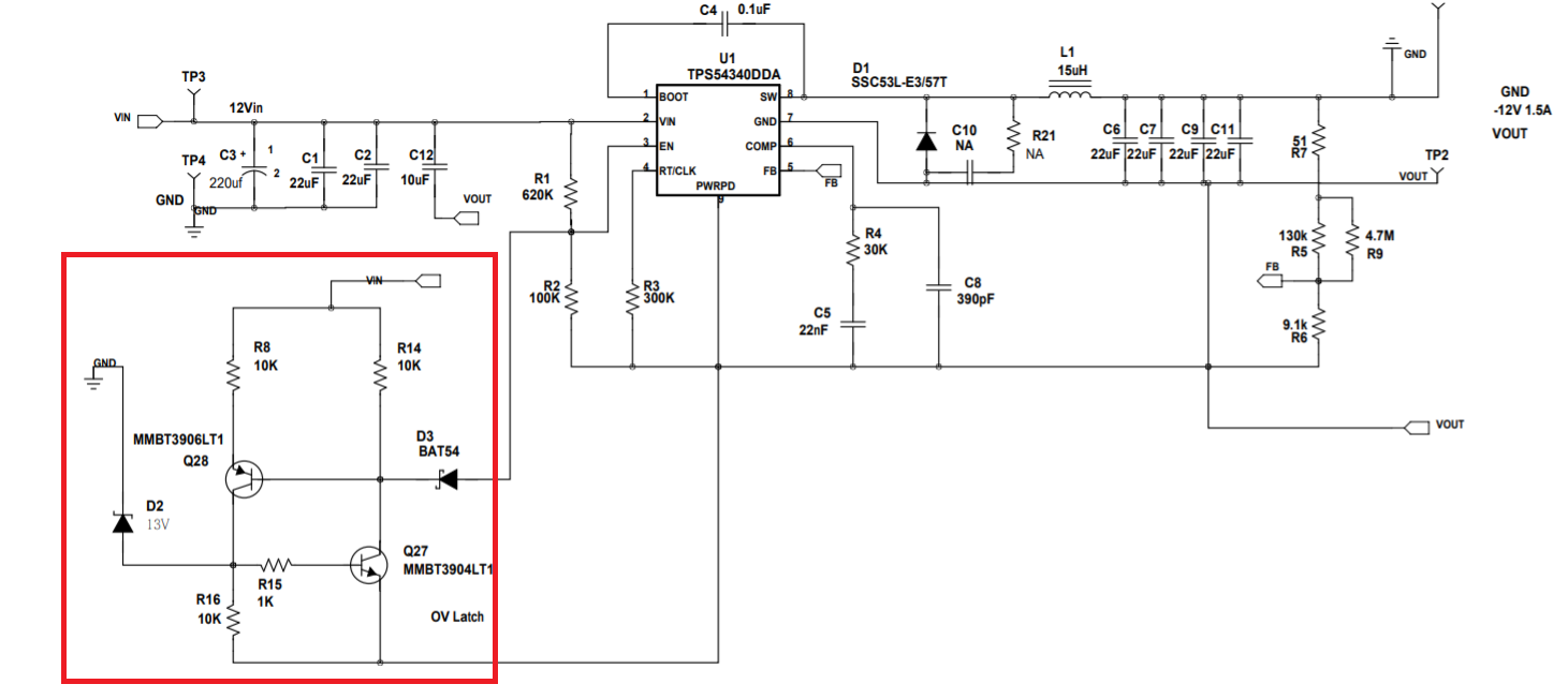
For PMP4369 design, I have checked the operation of enable/disable circuit block: 

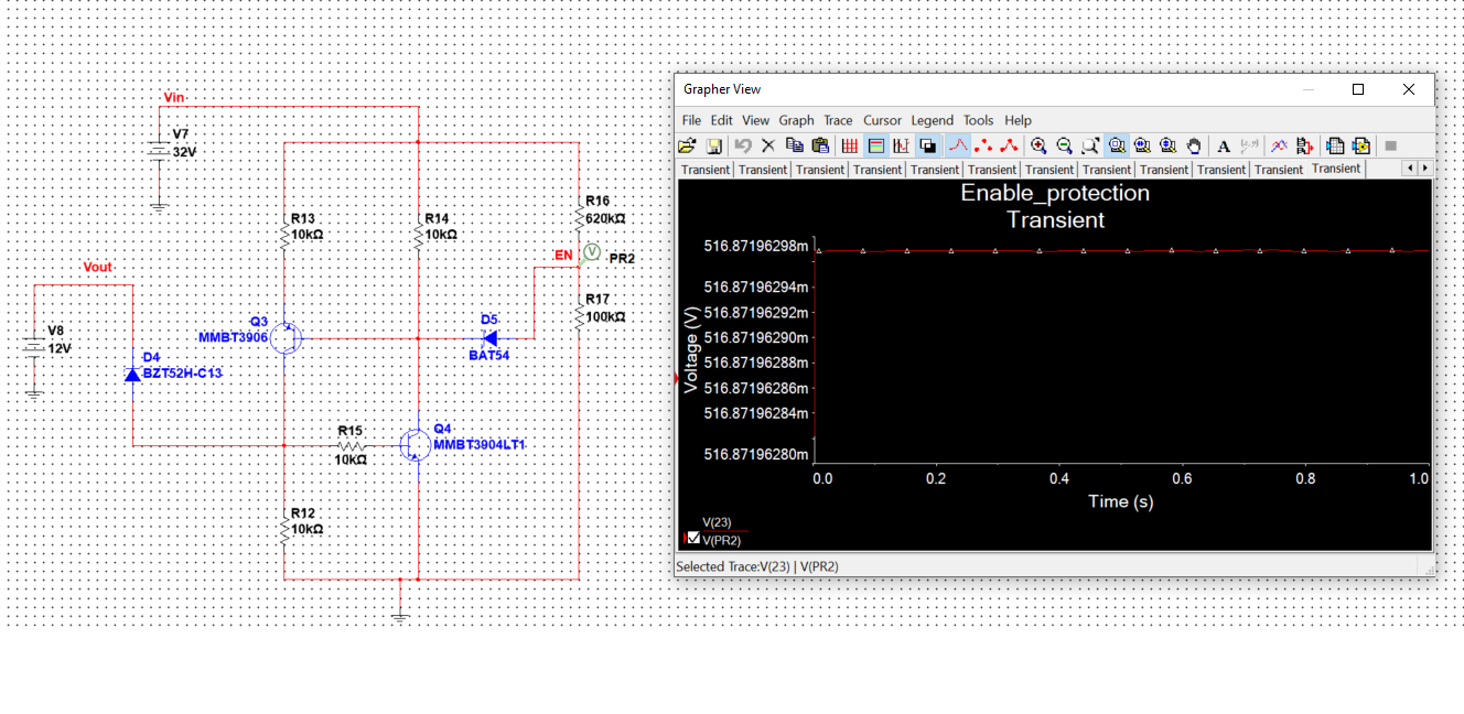
Theoretically, this circuit should disable the device when the output voltage is greater than 13V, but I am not very sure of the circuit operation as Vout is a negative voltage. I have launched a simulation and for negative output voltages the enable pin will see a negative voltage as well, thus, the device will be disabled. Maybe I am making a wrong reasoning.

Please, I need further details about this circuit operation. Thanks in advance for your support.

  • In addition, I have checked the TPS54340 datasheet and EN pin min. voltage is -0.3V, therefore, negative voltage are not suitable for this input pin.

    According to your schematic, the voltage on EN pin will be negative because Vout is negative. I think this block was thought for a buck converter with a positive Vout. In that case the circuit should be as follows:

    In this case I understand the operation of the circuit but in case you use the buck converter as a inverter, the circuit proposed does not work properly.

    Looking forward to hearing from you. 

  • HI Manuel,

    I would recommend you to read this app note to understand the Lavel Shifting Control for inverting Buck-Boost Topologies,

    http://www.tij.co.jp/jp/lit/an/slva540/slva540.pdf

    If you think my response answered your question then please close this thread. Thanks!

    Best Regards,

    Ankit Gupta

    Application Engineer.

  • Hi Manuel,

    I don't see any issues with level shifting circuit. At startup, the TPS54340 sees a Vin of 12 V with a reference to the system ground. Thus, the EN pin follows the same electrical characteristics outlined in the TPS54340 datasheet. The maximum turn on (logic high) voltage on the pin must be greater than 1.3 V. When the output of the inverting buck-boost is regulated to –12 V, the TPS54260’s “ground” reference becomes –12 V. If a level-shifting circuit is not added to reference the EN signal to –12 V, then the EN pin will see an overall potential of 1.3 V + 12 V = 13.3 V. This potential is more than the absolute maximum rating of 8.4 V which can easily damage the part. To prevent damage to the EN pin from overvoltage, the level-shifting circuit will output a potential of –12 V + 1.3 V = –10.7 V or greater to enable the TPS54340.

    Hence EN Pin won't see the negative voltage during startup or regulation. To understand the level shifting cicuit operation more comprohensively please read through these following TI app notes:

    1. http://www.ti.com/lit/an/snva856/snva856.pdf

    2. http://www.ti.com/lit/an/slva478b/slva478b.pdf

    3. http://www.tij.co.jp/jp/lit/an/slva540/slva540.pdf

    Hope this helps

    Best Regards,

    Ankit Gupta

    Application Engineer

  • Hello Ankit,

    now it is clear. Thanks a lot for your info and your kind response. Have a nice day.