


Hello
I made a half-bridge power supply like TI's LM5035 development board. The schematic is similar to the following:
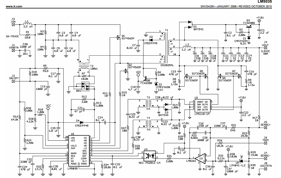
Produced 30 prototypes, 20 normal, 10 abnormalities.
When the power is turned on, the secondary synchronous rectifiers Q4~Q7, Q4 and Q5 are burned, and the gates of Q4 and Q5 have obvious black marks. Some of Q6 and Q7 are burnt, and some are still strong.
It seems that the synchronous rectification drive circuit is short-circuited, causing the Q4 and Q5 gates to burn out, and the DS terminal is short-circuited, and short-circuited with Q6 and Q7.
I suspect that it is a synchronous rectification drive problem. I removed the drive signal of Q4~Q7 and rectified it with the body diode. The circuit can work without load. But with the addition of synchronous rectification, the MOS is burned. I suspect that the synchronous rectification signal is abnormal, and it is normal to see a drive waveform. Very strange.
There is also a strange phenomenon, when only using body diode rectification, I brought a 1A load, the circuit can work, but the partial pressure between the primary R3, R4 is not uniform, not Vin/2, and the good prototype is partial pressure balanced. I measured the primary voltage divider resistor and capacitor. The resistance and capacitance are not much different. I measured the primary MOS drive signal LO and HO and found that the good drive signal is consistent. The duty cycle of the bad drive signal is one. Big one is small. I wondered, I don't know what caused this partial pressure? Due to the uneven voltage, the voltage on the secondary pin of the transformer, that is, the voltage at the left end of the output inductor L2 is also large and small. I only know that the phenomenon is abnormal, but I can't find the reason, but I don't know how to check it. ? Also please expert guidance, thank you!
