This thread has been locked.

If you have a related question, please click the "Ask a related question" button in the top right corner. The newly created question will be automatically linked to this question.

TPS54360: Use TPS54360 in the Buck-Boost Converter

Part Number: TPS54360

Hi team,

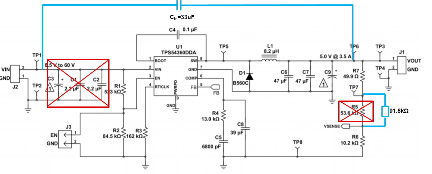
When I configure the TPS54360 EVM in a Buck_Boost converter which input voltage is 12V , output voltage is -8V and maximum output current is 2A. I meet some troubles. And I have make some changes in the TPS54360 EVM Board and the changes are shown below:

1.Change the Cin connection from Vin and ground to Vin and Vout as shown in the red and blue line;

2.Change the feedback resistor R5 to 91.8k to realize output voltage equal to -8V;

3.Add a 330uF output cap to the output terminal;

The problem is that with different load condition, the output of the converter will change a lot:

In the experiment, I use two 4ohm 250W resistors as the load.

1. When there is no load, the output voltage is -8V.

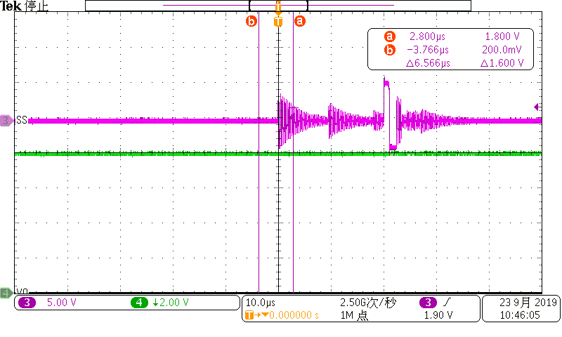
2. When the load is 8ohm resistor, the output voltage will drop to -4.8V or -3.62V.

When the output voltage is drop to -4.8V the SW waveform period is 3.326us and the on pulse time is 1.086us.

When the output voltage is drop to -3.82V the SW waveform period is 6.566us and the on pulse time is 1.4260us

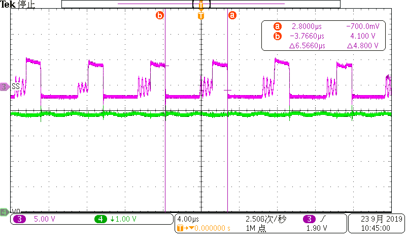
3. When the load is 4ohm resistor, the output voltage drop to -1.8V and the SW waveform period is 13.086us and the on pulse time is 1.526us.

All the waveform is shown in the figure below:Purple waveform is SW waveform and Green waveform is Vout.

no load with Vout=-8V.

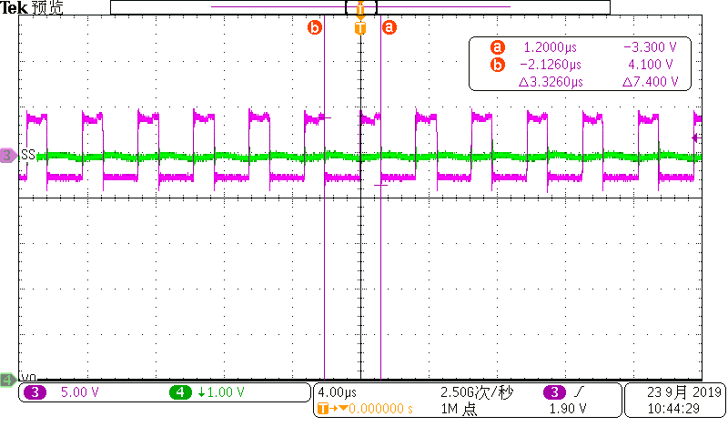
8ohm load with Vout=-4.8V.

8ohm load with Vout=-3.8V.

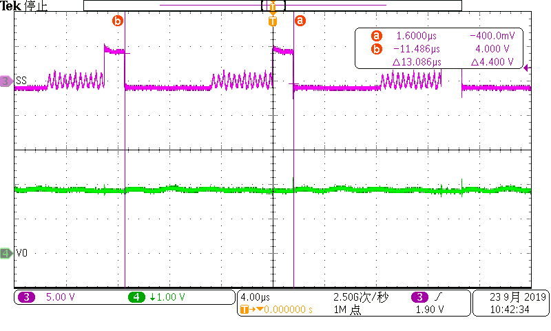
4ohm load with Vout=-1.8V.

So could you tell me how can I do to solve this problem and output a stable -8V at different load condition.

Thanks so much.

Best regards,

Lucas Niu

  • Hi Zhizhao,

    You need to add 0.1uF 50V cap on VIN pin2 and D1 GND

    How did you apply input voltage? the input voltage is about 5V on SW waveform, Vin 12V should be applied on J2 Pin2 and J1 Pin1 as the J1 Pin1 is system ground now, J1 Pin2 is -8V output. 

    Also make sure the input power supply has correct current limit setting.

  • Hi Andy,

    1.I have apply the 12V voltage on the J2 Pin2 and J1 Pin1. And the current limiting is enough to supply the load condition.

    2.And yesterday afternoon I re-solder the capacitor C1 and C2 on the previous position, which is similar as your suggestion, and the converter can work

    normally. However, for a conventional discrete buck-boost converter, this capacitor is not required. So could you tell me what is the role of adding this capacitor here?

    Thanks and best regards,

    Lucas Niu

  • Hi Lucas,

    In buck-boost conversion. there is also dis-continuous current with high di/dt in loop of  VIN pin---->SW----->D1---->PGND, so the high frequency bypassing capacitor between converter VIN pin and D1 GND (or converter PGND) is essential to reduce spike voltage on VIN pin and SW pin which may cause unstable operation.

  • Hi Andy,

    I understand what you mean. Thank you very much!

    Best Regards.

    Lucas Niu