This thread has been locked.

If you have a related question, please click the "Ask a related question" button in the top right corner. The newly created question will be automatically linked to this question.

BQ76940: Questions about CHG and DSG

Part Number: BQ76940

Good day,

I've got a few questions regarding charging and discharging;

Here is my setup for testing; I use 9x 220 ohm resistors in parallel to a 36V source to simulate the 9S Li-Ion batteries. No load connected. 

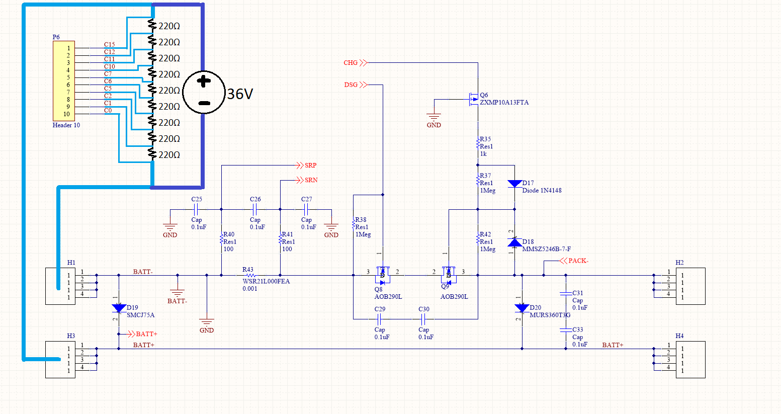
(1) In this setup, what should be the expected Vgs of the CHG/DSG FETs, is it 12V?

With all SYS_STAT faults clear and CHG/DSG bits set to 1, I get about Vgs = 7.07V on Q8 (DSG FET). On the other hand, I get Vgs = 0.73 on Q9 (CHG FET). To give more info, I measured Vgs on Q6 = -2.70V; Vr35 = 0.77V; Vr37 = 0.60, Vr42 = -0.73V.

(2) H2 and H4 are for connecting the Load OR the Charger, right?

  • Hi Robert,

    1. The typical voltage of VFETON (DSG or CHG when high) http://www.ti.com/document-viewer/BQ76940/datasheet/electrical-characteristics-slusbk25983#SLUSBK25983  will be 12V if REGSRC is high enough to allow regulation, or (VREGSRC - 1) V if it is not in regulation.  Since a normal circuit for REGSRC is a source follower referenced to VC5X, in the circuit sketched above VC5X might be ~ 12V (3 cells, 1/3 of the supply).  The source follower output will be about VGSth below, perhaps 2 or 3V below.  If a diode is included in the source like the EVM this may drop another 0.7 to 1 V to REGSRC.  So REGSRC may be 8-9V.  A 7V DSG high seems OK. CHG seems quite low.  If CHG is at a similar 7V, Q6 should be on.  R35's drop should be small, D17 might be 0.7V so Q9 Vgs should be around 6V.  Looking at your voltages, VR35 is .77V across the 1k, so 0.77 mA.  We might expect about 10 uA through R42.  R37 has diode D17 across it so has a forward diode drop.  VGSQ9 should be VR42  is 0.73, which looks like a diode drop.    Check to see if D18 is installed backward limiting the voltage and shorting the CHG pin pulling it down to about the VGSth of the Q6.

    2. Yes, load or charger attaches at H4 with respect to H2.  I forget that BATT+ is at the bottom of the figure sometimes.

  • D18 sure is installed backwards, thank you for that. Sorry for the careless mistake, details in SMD can sometimes be tricky. I'll re-solder tomorrow and give you an update.

    Some other questions;
    (1) Using electronic load, what current draw do you usually use for testing?

    (2) How do you induce short/over current to test the OCD/SCD faults and the protection?

  • Hi Robert,

    1. It really depends on what you want to do and the sense resistor value.  The EVM has a 1 mOhm sense resistor, the minimum OCD theshold is 8 mV, the minimum SCD threshold is 22 mV.  Those are 8 A and 22 A respectively, with tolerance.  So you need a capable supply and load to test trips.  
    SCD delay is short, you can sometimes get a trip from a power supply filter capacitor, but results vary.  Also keep in mind there are 2 types of short circuit event, one is a threshold crossing where the voltage does not change much but the threshold is crossed and the part protects.  The other is where the cells deliver full current collapsing the voltage and on protection have an inductive response.    If you are just wanting to see current in the coulomb counter a couple amps is usually OK.

    2. OCD can test with an electronic load.  An 8A setting with 36V is 288W, within the capability of a 300W load.  SCD might be tested with an electronic load if it will do a short, some recognize the power as beyond their capability and will not "short".   You can test with a resistor.  Some use a wire, an inline fuse is a good idea if for some reason the protection does not occur.  Protection is normally so fast the fuse does not heat or open.  Remember that arcing can occur and connections may stick or weld together, so use appropriate precautions. 

  • Re-soldered D18 properly, now the CHG and DSG Vgs reads 8.4V and 8.7V, respectively. Thank you very much!