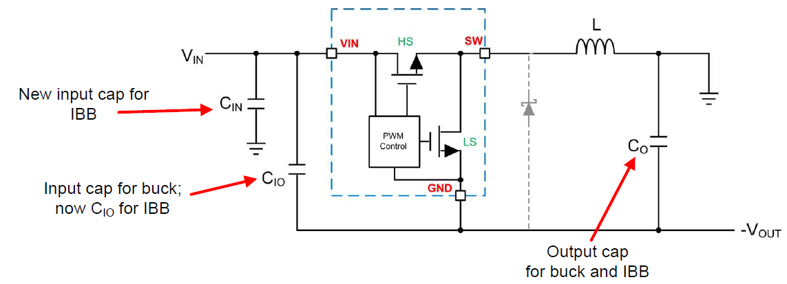
Hi team
Can I use the synchronous buck converter to do the inverting buck design like the design I do in the picture? if not, could you please explain why?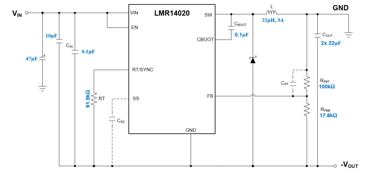
Hi team
Can I use the synchronous buck converter to do the inverting buck design like the design I do in the picture? if not, could you please explain why?