This thread has been locked.

If you have a related question, please click the "Ask a related question" button in the top right corner. The newly created question will be automatically linked to this question.

UCC27714: h bridge burns

Part Number: UCC27714
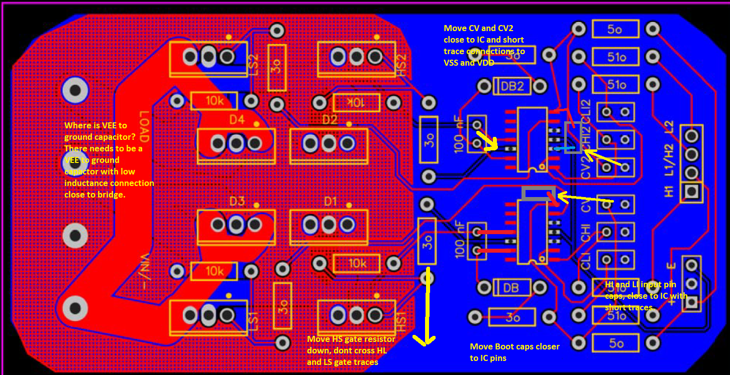
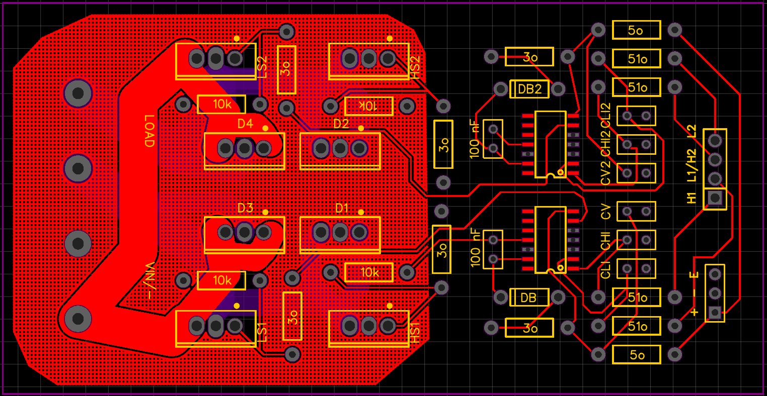
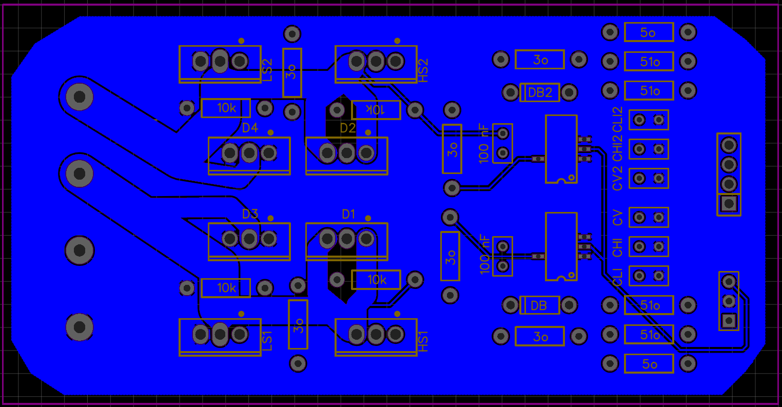
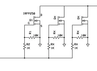
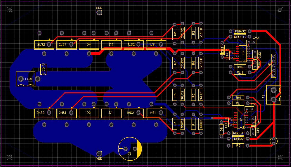
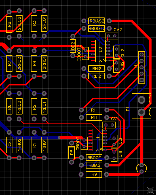
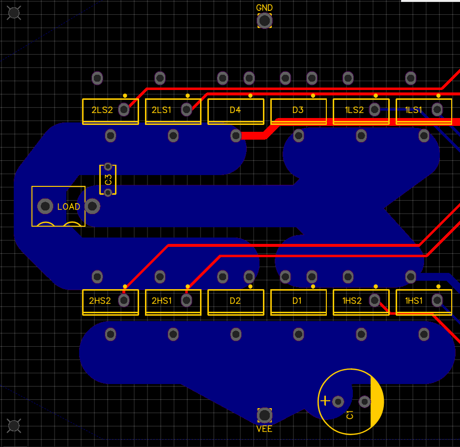
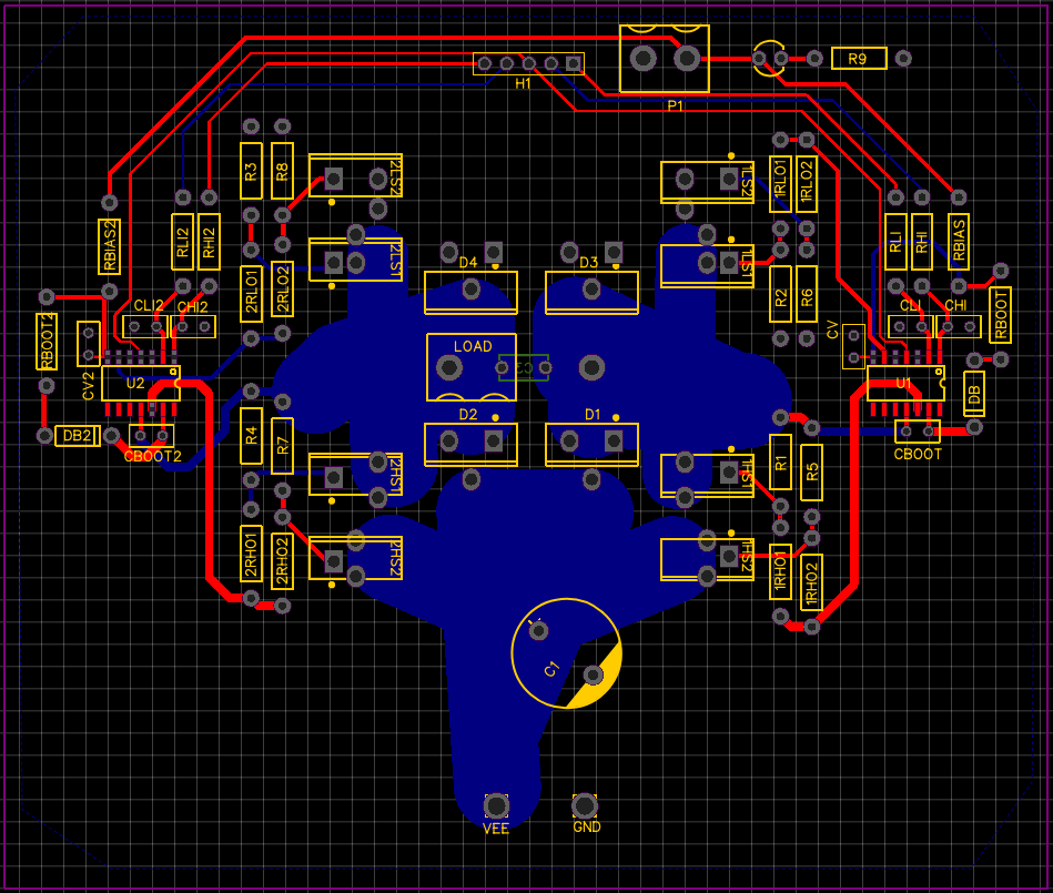
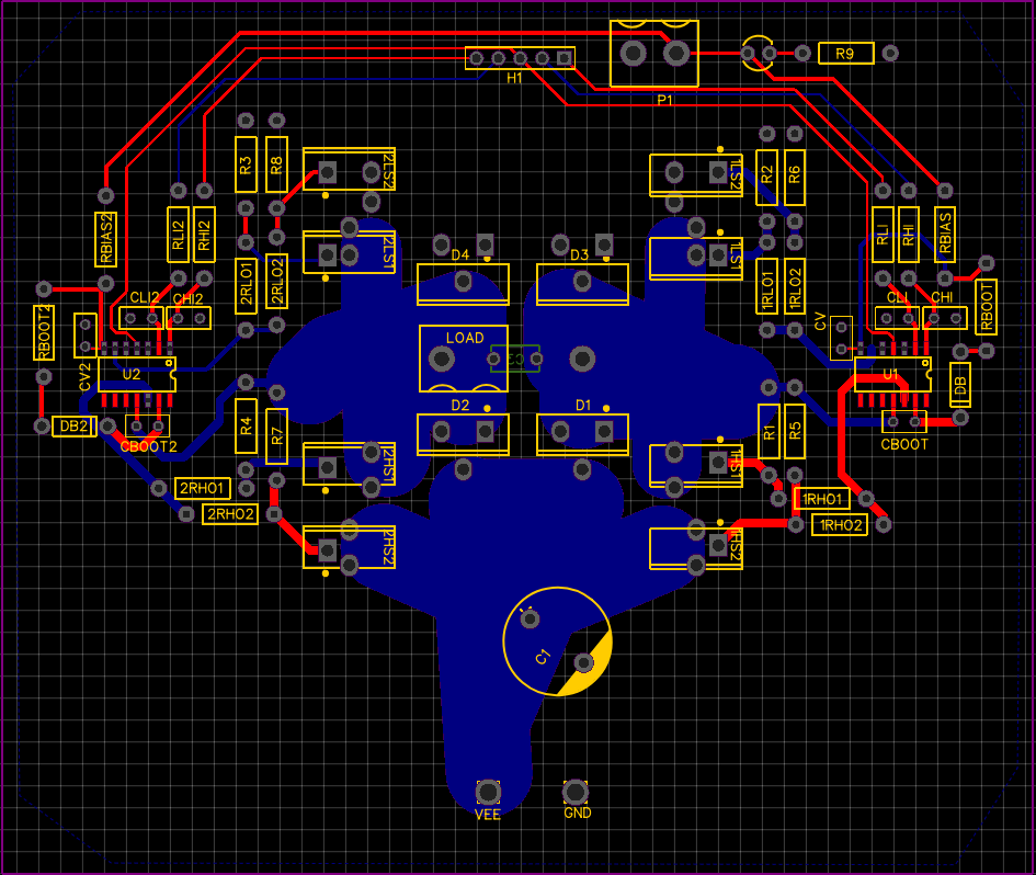
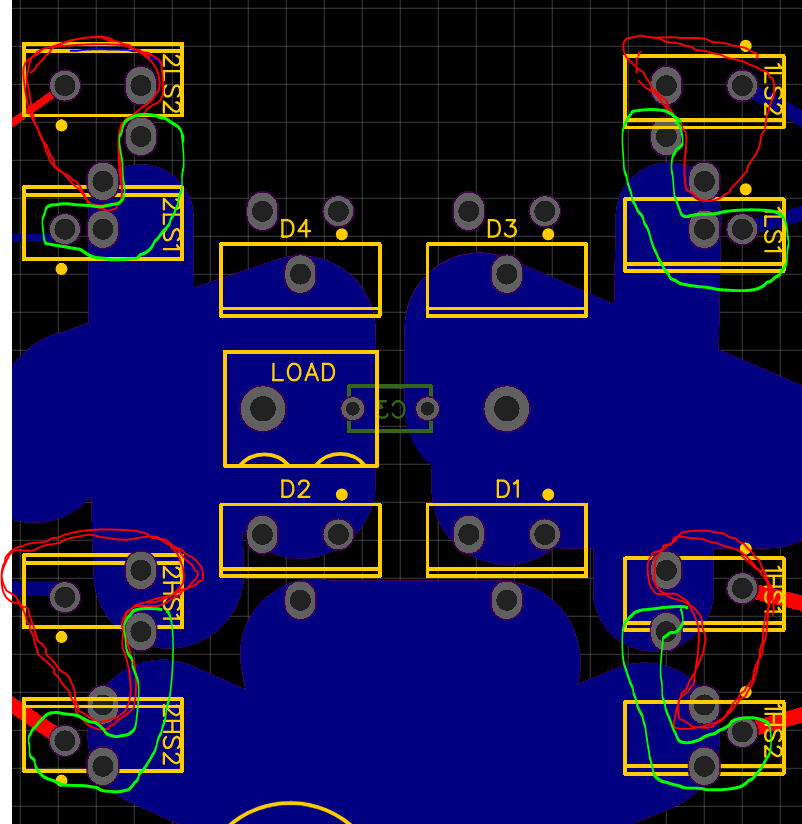
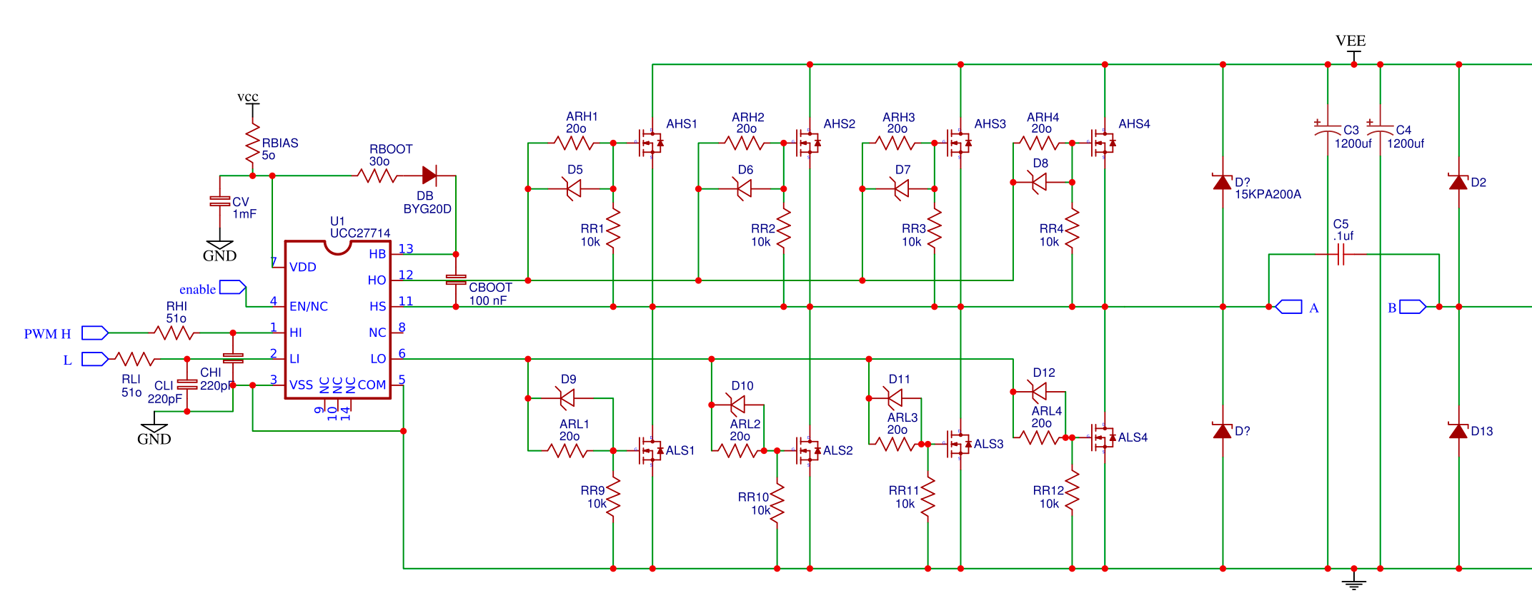
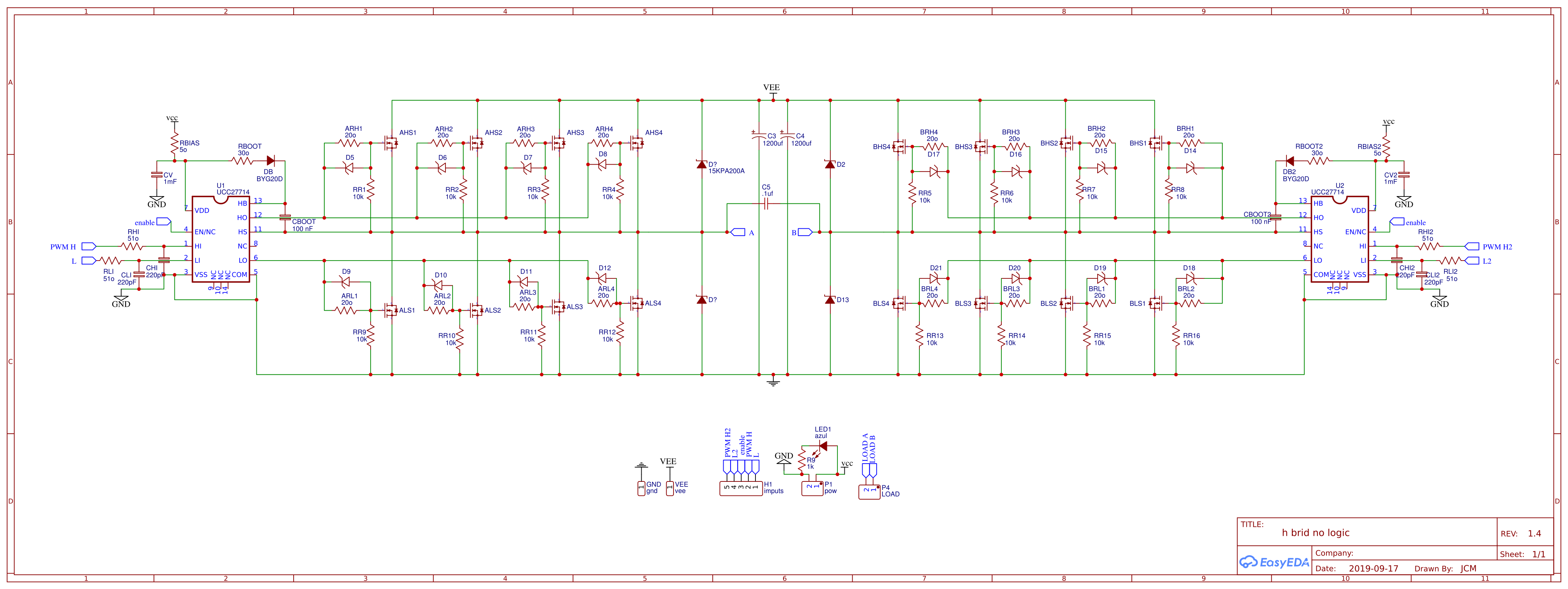
 Hello! my name is jesus and recently I have been working on the design of a high current h bridge, I have to say that I am a little novice and would greatly appreciate any help. Make a pcb with the design that I show you here (200v h bridge) with an arduino doing the logic, to generate the pwm and the dir. I don't know what could have happened, since once I connected the bridge and turned on enable the bridge h burned. I also attached the design of the pcb (5x10 cm) and a photo of how the bridge h.    

Please help me if you can!, I would be very grateful

  • Hello Jesus, 

    Thanks for reaching out.

    While we're reviewing your schematic, can you please share details of the issue you're experiencing with your half-bridge including operating conditions (VCC, VEE, Fsw, EN) during the issue, waveforms during normal operation. What specific IC's are failing? Are you having issues with both U1 and U2 or which one specifically?  Please include all components that did "burn". 

    Regards,

    -Mamadou

  • Mamadou Diallo said:

    Hello Jesus, 

    Thanks for reaching out.

    While we're reviewing your schematic, can you please share details of the issue you're experiencing with your half-bridge including operating conditions (VCC, VEE, Fsw, EN) during the issue, waveforms during normal operation. What specific IC's are failing? Are you having issues with both U1 and U2 or which one specifically?  Please include all components that did "burn". 

    Regards,

    -Mamadou

    Hi mamadou! thanks for answering, I experienced the problem when I turned on the enable, I was controlling the control signals through an arduino, when I turned on the enable the low side resistances of the bridge blews up (RLO and RLO2) and the mosfet HS1 also shows signs of burn. The operating conditions were VEE = 84v, VCC for the arduino and the ucc27714 was 12v, the PWM set it to 31kHz, I am not sure if it was a problem of the ICs or a bad design ... If you could shed some light on the matter would be eternally grateful. The motor I am trying to control is something special and needs a very high switching frequency. I think you may need a capacitor between VEE and GND

    If you need any more information I will be happy to give it to you, I also attached the list of components.

    Resistors:
    RBIAS 5ohm 1/4W
    RBOOT 3 ohm 1/4W
    RHI 51ohm 1/4W
    RLI 51 ohm 1/4W
    RHO 3ohm 1W
    R1 10Kohm 1W
    RLO 3ohm 1W
    R2 10Kohm 1W

    Capacitors:
    CV 1microF
    CBOOT 100nf
    CLI 220 pf
    CHI 220 pf


    MOSFETS IPP110N20NA
    FW DIODES MBR20200CT
    DBOOT BYV26C


  • Hello Jesus,

    I work with Mamadou supporting the 600V half bridge drivers and I will address the questions with the information provided so far.

    On the schematic, most of the component values for the driver look OK regarding VDD capacitance, boot capacitance, boot diode and input filter. With a 100nF boot capacitor, I would increase the series boot resistance to ~22 Ohms to limit the initial boot cap charging dV/dt.

    Also for the gate resistance, since you are having some issues now, I would increase the gate resistance to at least 10 Ohms for now.

    for the layout I don have some concerns which could lead to functional issues. The CV and CV2 need to be close to the IC VDD and VSS pins and have short trace connections. The existing layout has long traces. The boot capacitors are much better, but I would recommend moving closer to the IC pins. The LI and HI filter capacitors should also be close to the IC pins with short traces. In general, anytime there is a bypass capacitor, place the cap close to the IC and connect with short traces as possible.

    The gate resistor for HS1 should be moved down so that the LS1 trace does not cross the HS1 driver output trace. This could lead to noise coupling on the driver outputs. I do not see a filter or bulk capacitance for the high voltage VEE to ground. There needs to be a bypass capacitance relatively close to the bridge power devices to minimize the trace inductance in the high current path.

    For the troubleshooting. I would move the capacitors close to the IC pins as described, and add filter capacitance to the VEE and ground. At least ceramic HF filter capacitance. With your test sequence do the PWM signals start after the Enable to the drivers? I would make sure there is a "safe" start sequence where the PWM signal duty cycle is known and not random on the enable of the power train. Confirm the control and driver signals in a condition with lower VEE voltage, or with VEE at 0 to make sure there is not a conflict in the driver control, and that the driver outputs are operating as expected.

    Below is the layout with some comments.

    Confirm if this addresses your questions are you can post additional questions on this thread.

    Regards,

  • Thank you very much Richard, your answer has helped me a lot, as I said I am a little newbie yet and I did not take these questions into account, I am very grateful for your collaboration, I will make the modifications you indicate and I will try. On the other hand do you see well the treatment of the VEE tracks? Would you widen these traks? It is only 200v that must be supported, not the 600 for which the ucc27714 is prepared.

    Thank you again, if you have any other recommendation it will be very well received. When I solve these questions I will post the result so that another person can use them if needed.

    Thank you very much for everything again! Greetings.

  • Hello Jesus,

    We are willing to help with any issues that you have in your designs using our TI products. I may have omitted the comment earlier. That I would suggest wider trace widths for the driver output connections,  and VDD and HB capacitor connections. I cannot see all of the power FET bridge connections so I cannot comment for all of these connections. The top trace connecting the diodes D3 and D4 to the FETS looks capable of high current. I am not sure what current, peak and average will be in the power train.

    Confirm if this addresses your questions to look at hardware operation improvements. You can post additional questions on this thread as needed.

    Regards,

  • Hi Richard, thanks again, I really appreciate your help, I will make the changes you recommend and I will publish the result, so if all is well everyone who needs it can use the design. Meanwhile attached screenshots of the top and bottom layer in case you see any fault.

    Thanks again, regards!

  • The maximum current would be 200v and 88A determined by the MOSFETS.

    Another question, could I place mosfets in parallel this way? with their respective modifications of course

  • Hello Jesus,

    Sorry for some delay on the latest post. Yes, the MOSFETs can be paralleled and you are showing the recommended configuration where each MOSFET has individual resistors in series with the driver output. I assume you are showing the 1K as a placeholder. For the gate source resistor be careful not to have too low a value on the high side driver as the gate to source resistance will discharge the HB capacitor. For the series resistance to the gate driver output I would recommend a range of 20 Ohms to 100 Ohms to be determined by the switching time and Vds dV/dt in the application.

    Confirm if this addresses your questions, or you can post additional questions on the thread.

    Regards,

  • Querido Richard, gracias por su respuesta, no te preocupes por el delay. las resistencias de 1k eran de ejemplo, finalmente los valores para RHO and RLO son de 20 ohm ya que necesito tiempos de conmutacion bastante rapidos, como de 30kHz o algo mas, ves bien este valor de resistencias? Tambien he incluido condensadores de bypass entre VEE y GND y entre LOADA y LOADB. Para finalizar te traigo unos screenshots del nuevo diseño de PCB y el nuevo esquematico donde se pueden observar los valores de todos los componentes. Que te parece el nuevo diseño? Espero que se vea claro todo el ruteo, si tienes cualquier duda estare encantado de aclararla.
    PD: all GND is connected through a copper area that is hidden
    Regards, Jesus.
  • Hello Jesus,

    The layout of the components supporting the UCC27714 looks improved with the bypass capacitors close to the IC pins. The gate resistance of 20 Ohms should be a good initial value, and you can evaluate in the hardware testing regarding the switch node dV/dt and any voltage spikes and overshoot. Increasing the gate resistance can hep reduce voltage spikes. The trace lengths to the 2LS and 2HS are still very long, and that trace inductance can cause significant Vgs rining and overshoot.

    I would suggest taking the gate driver and all support components, and the gate drive resistors and move them to the left, and make the layout more compact which will result in shorter gate driver output traces. If you move the gate drive series resistors close to the power Mosfets, the gate drivers and support components can be moved much closer to the Mosfets.

    The traces to the 2LS and 2HS will still be a little long, if you make the changes. On suggestion that helps with long gate drive traces, is to add capacitance from the MOSFET gate to source very close to the MOSFET. This will help reduce the Vgs ringing significantly.

    Confirm if this addresses your concerns or you can post more questions on this thread.

    Regards,

  • Hey Richard! What do you think? Better??

    Thanks for everything again!! you are a great company.

    Regards, Jesus

  • Hello Jesus,

    That layout looks a lot better regarding reducing the gate drive trace lengths. The only small comment I have is if you rotate IRHO1/IRHO2 and 2RHO1/2RHO2 90 degrees you can shorten the trace length from the driver HO outputs to the resistors.

    Also I would swap locations of 1RLO1/IRLO2 with R2/R6 to make the low side traces shorter like you have on the other side. Those couple of small changes are the only comment I have.

    Confirm if this answers your questions, or you can post additional questions on this thread.

    Regards,

  • Hi Richard! Thank you for the quick response I appreciate it very much.
    Finally I modified the design according to your small comments, the result is this.

    Finally, and I hope not to be very unbearable, would it be advisable to add capacitors between the door and the source to reduce the Vgs ringing?

  • Hello Jesus,

    The gate drive routing and driver components looks much better that the initial plots. There is one thing, I did not look at close initially but you need to check.

    Check the gate, drain and source connections of all of the MOSFETs. It does not look as it should and the pins placement for the MOSFETs looks different than usual. It looks like there is 2 Mosfets in parallel for each of the low side and high side, but the routing does not seem the drain and source are in parallel.

    Confirm if this addresses your questions or you can post additional questions on this thread.

    Regards,

  • Yes, it is because I modified the place of the pins to be able to make the tracks thicker, I attached a photo in detail

    Thanks again, I'm really grateful for your help.

    Regards, Jesus

  • Hello Jesus,

    Thanks for the clarification. If you have confirmed the power device connection, then I think the layout looks good.

    You should be able to have the power train operate as you expect, you may need to optimize switching speed and gate resistors once you start testing the new board.

    Confirm if this addresses your questions, or you can post additional questions on this thread.

    Regards,

  • Hi Richard, thanks to you for the help, I am very grateful. Right now I am waiting for the pcbs, I think they will arrive next week and then I will start testing, I will post them of course, so this thread will be more valuable.

    To optimize the switching speed, I will need to reduce the resistance of the gates, right?

    Regards, Jesus

  • Hello Jesus,

    From the schematic, I can't tell if the gate resistor is 3 Ohms or 30 Ohms. I doubt you will need to reduce from 3 Ohms, if it is 30 Ohms you can see if the voltage peaks and spikes are OK, and reduce the gate resistance to reduce switching times.

    I would start with a higher gate resistance value on initial test, 20 to 30 Ohms just to confirm the waveforms look OK.

    Confirm if this addresses your questions, or you can post additional questions on this thread.

    Regards,

  • Hi Richard! I hope you are well.
    Finally I assemble the plcb and everything went well for a few minutes (2 min) after an exploded low-sided mosfet (1LS1), the resistance of the gate was 22 ohm, for the rest everything as described in the schematic. Can you think of any idea what could have happened? I don't know if it will influence but I only applied PWM on the high side, while on the low side only a HIGH signal.

    Thanks for everything in advance, I attached some images.

    Regards, Jesus.

  • Hello Jesus,

    I see the MOSFET's do not have heatsinks, do you expect low power dissipation in the MOSFET's and diodes in the power train? If the power dissipation is not low, the MOSFET's without heatsinks will likely have high temperature rise.

    Since you can run for some time, without failure, I would run the board and monitor the temperature of the power devices for <2 minutes (before failure issues) and see if the temp rise is high.

    Also, when you say you are running the PWM on the high side, and low side is high (DC). Is this running HS1 with PWM and LS2 with DC, or HS2 PWM and LS1 DC? IF you run the HS1 and LS1 for example at the same time there will be high current shoot thru on the MOSFET bridge.

    Confirm that LS1/HS1 are not on at the same time, also for HS2/LS2. I would monitor temp rise on the power devices. If these concerns look OK Please provide some waveforms of the operation. Run the unit for short time to avoid failing.

    Record HI, LI, HO-HS, and LO. Record HI, LI, MOSFET switch node (HS), LO. Record several switching cycles, and also zoom in to one switching cycle to see the switching time details.

    Confirm if this addresses your concerns, or you can post additional questions on this thread.

    Regards,

  • Hi Richard! Thanks again for responding so quickly.

    Yes, the mosfets do not have heatsinks, it is a design flaw, at this moment I am designing the PCB again so that it has capacity for heatsinks. I have found some schematics of an open source project, the OSCM (www.robotpower.com/.../osmc_info.html) and I am being guided by them, I have decided to change the mosfets for some stronger ones like these (IRFP4668PbF) With better RDS (on) and 130A Id, I have also included TVS diodes (15KPA200A) replacing the freewheling diodes and leaving that task to the built-in diodes of the mosfets. I leave a screenshot to be clearer.
    What do you think about these changes?

    On the other hand I am not turning on AHS1 and ALS1 or BHS1 and BLS1 (these names refer to the new names that appear in the new schematic), I am just doing this AHS1 (pwm) BLS1 (HIGH) and the opposite for the change of direction BHS1 (PWM) ALS1 (HIGH), I'm sorry I didn't explain myself well in the previous post.

    When I have designed the new plate and everything is correct I will take measurements with the oscilloscope

    Thanks for everything again Richard! Regards.