This thread has been locked.

If you have a related question, please click the "Ask a related question" button in the top right corner. The newly created question will be automatically linked to this question.

LM74700-Q1: Circuit for LM74700-Q1 full bridge rectifier

Part Number: LM74700-Q1
Other Parts Discussed in Thread: LM5051

Hello,

I saw on a previous post involving Kari and Hiroshi that there was an circuit example using the LM74700 for full bridge rectification. I know there are some problems with the ground pin as the phases dip below ground. I'd love to see if there was a workaround for this. Could you please share the schematic?

Much appreciated.

Troy


  • Hi

    For the two High side diodes, LM74700 can be used.

    However for the low side two diodes, please use LM5051 (low side ORing) controller.

    Regards,

    Kari.

  • Kari-san,

    Thank you for your advice.

    Can you give me the cct. with detail controlling connections.

    And this fullbridge cct. can be used for input DC400V bus and DC48V output LLC circuit  as secondary rect.?

    H.DOI

  • Kari,

    I noticed that the LM74700 has a "Regulation max sink current" of only 26 microamperes, which is very small for our application. We have four top-side 1.6 mOhm, 39 nC gate-charge MOSFETs switching 40 amperes at 3500 Hz.  Do you see a problem with using the LM74700 for this purpose?

    THE LM74700 has a fast turn off current of 2370 mA. But this pull down current only takes effect when there is 27 amperes going in the other direction. Is this going to be a problem?

    Best,
    Troy

  • Kari-san, Troy-san,

    The Load is  DC48V  73A.

    Is it OK ?

  • Hello Troy,

    Regulation sink current is used to regulate the Vsd voltage to 20mV during normal operation and if the current drawn on the MOSFET exceeds 50mV/RdsON, the MOSFET is fully enhanced.

    Regulation sink current is not relevant for the bridge rectifier, because turn off is triggered by a relatively fast switching (AC) input (3.5KHz). Regulation sink current is relevant to turn off during a slow ramping down input voltage.

    Regarding the gate drive capabiility of LM747000, it has 300uA charge pump current and with 300uA at 3.5KHz, it can support 300uA/3500Hz = 85.7nC of gate charge. Worst case 162uA charge pump current leads to 46nC of gate charge.

    Fast turn off current of 2.37A is suffcient to pull down the 4x 1.6mohm MOSFETs with 39nC. Yes, it will need 27.5A of peak reverse current to turn off MOSFETs, but this is only a transient current for 1us. (including the time to discharge gate charge = (39nC *4) / 2.37A = 65ns, comparator time is 0.75us maximum)

    I am putting together the reference schematic and will share it tomorrow or early next week.

    Let me know if you need it earlier.

    Regards,
    Kari.

  • Kari-san,

    It's not 3.5kHz .

    Primary LLC frequency is 50kHz(heavy load) to 200kHz(light load).

    TTL secondary  load is 3.5kW.

    H.DOI

  • Hello 

    LM74700 is not suitable to operate beyond 50KHz of AC input, as the rectification can not happen.

    Also we recommend only for AC pk-pk about 45V application.

    Regards,

    Kari/

  • Kari-san,

    Thank you very much.
    This 5M/year x4 pcs demand seems to be consulted with other IC manufacturers.

  • Hi Kari,

    Would you mind sharing that schematic? Also, has it been validated / tested for use as a rectifier?

    Best regards,

    Troy

  • Hi Troy,

    We have a proposal of the schematic, but have not verified at high currents.

    Simulation can be run to verify the schematic.

    We would need some more time to get back.

    Apologies for the long time wait, but certainly this is taking some additional time.

    Regards,

    Kari.

  • Hello Troy,

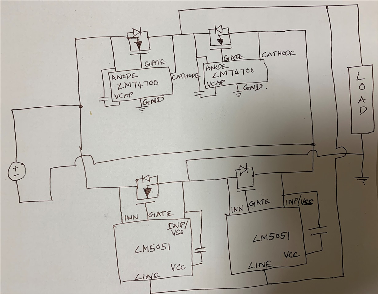
    For operation above 36V (rectified output), schematic proposal is attached which uses LM74700 for high side MOSFET control and LM5051 for low side MOSFET control. Kindly bear with the hand drawn schematic, as creating one with tools is taking time.

    Let me know if this works for your need, certainly this circuit will not work for very high frequencies, supported AC input frequency = (Charge Pump Current) / (MOSFET Gate Charge). Supported input AC peak to peak voltage = 65V and rectified output minimum voltage is 36V. However for using with lower rectified output requirements, LM5051 portion of the schematic needs modificaiton. LINE pin does not work below 36V, instead need to use resistor between ICs VCC pin and rectified output (+ve voltage of load), as detailed in datasheet page 13 (figure attached below)

    We would encourage you to simulate using the simulation models available on the product folder pages.

    Vcc pin config for operation (rectified output voltage) below 36V is shown below.

    Bridge rectifier usage: Instead of connecting the resistor to GND as shown in figure 29, connect resistor to rectified output.

    Regards,

    Kari.

  • Kari,

    Thank you so much. In previous posts you had mentioned that the GND pin on the LM74700 required careful consideration. I presume this is due to the fact that source/anode pin on the high side MOSFET drops below GND, sometimes by as much as 0.7 V. 

    1) Do you have any suggestions for how to prevent problems resulting from this fact?

    2) Have you tested this design before? I just want to make sure before I begin creating my PCB.

    Thank you,

    Troy

  • Hello Troy,

    Yes the 0.7V diode drop in the GND pin can be a concern and to avoide issues, Vs pin of LM5050 and Vcc pin of LM5051 needs proper decoupling.

    Please note that we have not tested the full bridge rectifier circuit, the schematic was a proposal.

    You can verify the schematic using the PSPICE models available on the product folder webpage.

    Further I believe, I have answered your questions. Let us know if you have further questions.

    Otherwise, if you think your questions are answered, click "this resolved my issue" button at the end of the thread.

    Regards,

    Kari.