


Hi TI Team,
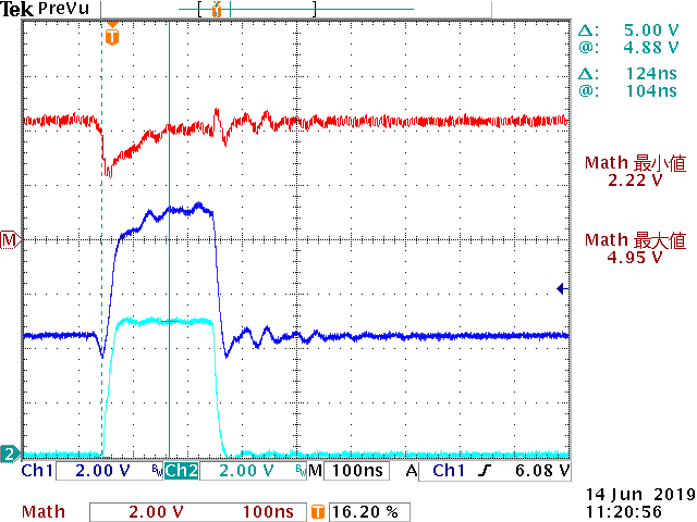
About TPS543B20 boostrap resistor value, TI recommends 0 ~ 10Ω.
Our design uses 22Ω + 0.1uF, to reduce spike.
Is there is any concern about the operation with this value?
Best Regards
Naim
Hi TI Team,
About TPS543B20 boostrap resistor value, TI recommends 0 ~ 10Ω.
Our design uses 22Ω + 0.1uF, to reduce spike.
Is there is any concern about the operation with this value?
Best Regards
Naim

