This thread has been locked.

If you have a related question, please click the "Ask a related question" button in the top right corner. The newly created question will be automatically linked to this question.

TPS61200: Failure with Vin >= 4.2V

Part Number: TPS61200
Other Parts Discussed in Thread: TPS61099

We have a product that has been in production for multiple years that use 2 of the TPS61200 boost converters.  One is set for a Vout of 3.37V (R1 = 1M, R2 = 174K) output while the other is set for 5.05V (R1 = 1M, R2 = 110K).  Currently our product is powered by either 2 alkaline batteries (3V max) or one primary lithium cell (3.6V max).  With this configuration, everything is working well.

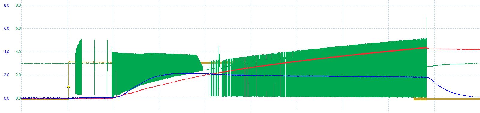
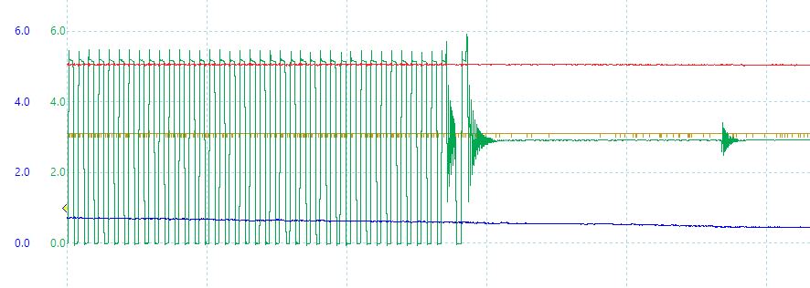
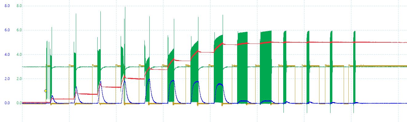
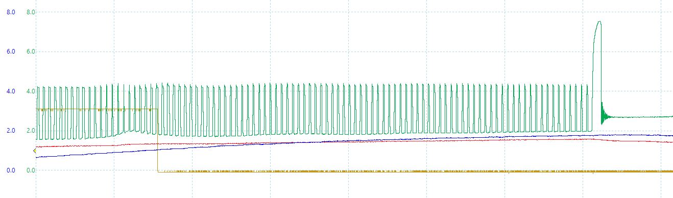
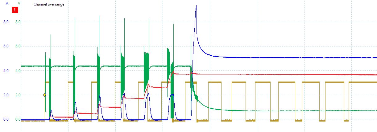
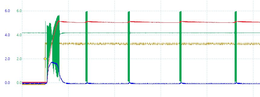
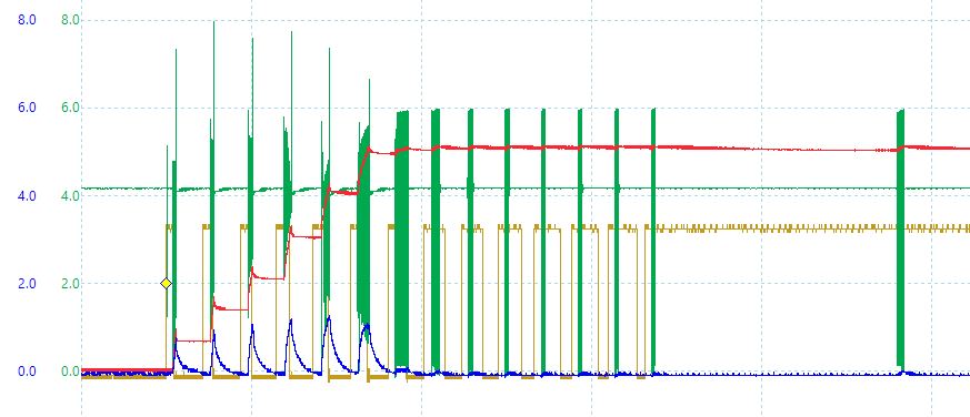
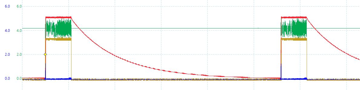
Recently we decided to switch to a rechargeable lithium-ion cell for the input source (4.2V max).  In my testing, I have been able to "kill" the TPS6100 device that is set for a 5V output.  On multiple boards, when the input supply is set to 4.2 - 4.3V, the TPS61200 shorts outs.  Sometimes this takes multiple power cycles.  So far, this has only happened when using a benchtop power supply and not the actual lithium-ion cell.  I suspect that the lithium cells never reach a full 4.2V.  I am using an Agilent power supply and have verified that there is no overshoot.  We also have a reverse and over-voltage protection circuit in series between the battery input and the Vin pin of the TPS61200 devices.  The over-voltage threshold is set at 5V.  The Vin of both the 5V and 3.3V power supplies are tied together.  It is only the 5V supply, however, that is having issues.

Supply 1
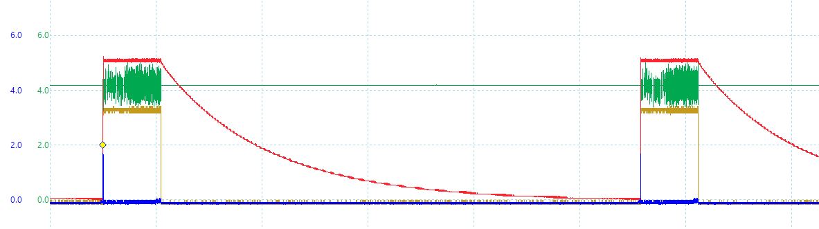
TPS61200 set for Vout = 5.05V
The enable pin is under software control.  It is set true about 3 seconds after power is applied to the device.
There is approximately 450uF of capacitance on the output.  20uF is directly connected to the Vout pin while the remainder is near the load.

Supply 2
TPS61200 set for Vout = 3.37V
The enable pin is tied to Vin.
There is 20uF of capacitance directly connected to the Vout pin.

There is 1320uF of capacitance on the input to both supplies.

I have attached the schematic and layout.  On the layout snippet, the ground fill is suppressed.

Do you know why I might see different operation with an input voltage of 4.2V rather than 3.6V or 3.0V?  Since the failure mode seems to be related to the input voltage, why am I only experiencing failures with the TPS61200 that is setup for Vout = 5.05V?  Both devices are connected to the same input voltage.  The layout for both parts is also identical.

When the 5V supply is enabled, the only load is the capacitors on the output.  The actual load is turned on about a second later.

Thank you for your help -

Scott

  • Hi Scott:

    Thanks for asking.

    Firstly, please make sure there is no soldiering issue and all the components are good before the test. (Including new TPS61200)

    After that, please do the test U1 follow:

    1. Power on with 3.6V Vin, after check everything is fine then enable the converter and keep it. Then catch the waveform of Vin, Vout, L, Vaux.

    2. Then slowly rise the Vin, to check when the issue happen. And catch the wave form again.

    3. After that, decrease the Vin back to 3.6V, to see if the converter could work well.

    It's better to catch the waveform with details of switching cycle and overview for the transient.

  • Thank you for the quick reply.  I will work on getting you some plots.  Prior to that, I still have some questions.

    We have 1000's of devices out in the field that are working fine with a Vin between 1.6 - 3.6V.  What would make the TPS61200 part more susceptible to damage with a higher Vin?  4.2V is still below the 5.5V maximum rating of the part.

    When the TPS61200 part fails, it is right after it is enabled. The part does not seem to fail once it is up and running and the output is stable.  It seems to be an issue only during startup.

    Would having a large amount of capacitance (~450uF) on the output and a higher input voltage create higher currents and possible excessive voltage spikes on the inductor switch pin (SW)?

    Thanks for your help -

    Scott

  • Hi Scott:

    Does the issue only happen during the startup? What about rise the Vin from 3.6V to 4.2V with converter keep enable?Please add a test without big Cout, to check if the issue is gone.

    It's better to do deep analysis after the test and geting the waveform. Thanks for your kind understand.

  • The issue happens immediately after the TPS61200 is enabled.

    If Vin is set to 3.6V and then the part is enabled, it will work fine.  Once the TPS61200 is up and running I can sweep Vin from 2.0 to 4.5V without any issues. It seems to be a start up issue.

    Despite this part claiming to have a soft-start feature, it does not work well.  The part will draw considerable current (>2A) to ramp the output voltage as quickly as possible.  We confirmed this issue with a TI application engineer (Jasper Li) back in early 2018.  This can also be duplicated on the TI evaluation board.  This issue is exacerbated when there is additional capacitance on Vout.

    When using alkaline batteries, this high inrush current would sometimes pull the input voltage down (due to the internal resistance of the batteries) to the point where our product would reset.  To solve this, we pulse the enable line a few times over a 10msec period before setting it high permanently.  This lowers the peak inrush current.  When we discussed this work-around with TI last time, they indicated that it shouldn't cause any harm to the part.  Maybe this isn't the case with the higher input voltage.

    With the higher input voltage (4.2V), I'm wondering if we are getting even higher currents in the inductor during the ramp up phase.  When the internal inductor switch turns off maybe we are getting a large inductive kickback voltage that is killing the part.

    I will try to get some extra boards to test with.  Unfortunately, I do not have any extra working boards and our lab technician is out sick.  The TPS61200 is not an easy part to rework.

    Thanks for your help -

    Scott

  • I have some plots that I'd like to go over with you.  I was not using the highest resolution / highest speed oscilloscope so the values should be treated more as relative than absolute.

    My biggest area of concern is a voltage overshoot on the "L" pin when the enable pin is de-asserted while the output voltage is still ramping up.

    I have scope and current probes at the locations show in the schematic below.

    The channels on the scope traces below are configured as follows.

    Color Pin Notes
    Blue Vin Current probe on the input to the circuit board, 2A/div
    Red Vout 2V/div
    Green L 2V/div
    Yellow EN 2V/div

    In the following plots, the input voltage (Vin) is set a 3.0V.  The output voltage (Vout) of the TPS61200 is set at approximately 5V.

    Plot 1
    Horizontal scale - 200usec/div
    The enable pin is disabled while Vout of the TPS61200 is still ramping up and the device is still actively switching.  The device is disabled prior to Vout reaching the 5V set point.  During the Vout ramp up phase, the current draw of the device is around 2A.

    Plot 2
    Horizontal scale - 10usec/div
    Zoomed in view of plot 1 showing the large voltage spike on the shutoff of the inductor switching.

    Questions:
    Why is there such a large voltage overshoot on the final pulse?
    Why does it take 56usec for the device to stop switching after the enable has been de-asserted?

    Plot 3
    Horizontal scale - 250usec/div
    In this plot the device is enabled indefinitely.  Once Vout reaches the set point (5V) the switching stops.  The device is configured in power save mode.  There is not a large voltage overshoot like in the previous plots.

    Plot 4
    Horizontal scale - 10usec/div
    Zoomed in view of plot 3 showing the final pulses of the inductor switching.

    Because the TPS61200 draws so much current during startup, we pulse the enable line a few times to spread out the inrush current.  This was required since the large 2A current draw would pull down the voltage of the attached alkaline batteries.  If the batteries were partially discharged, the voltage drop could be enough to reset our processor.  We have been using this approach for over 2 years without issue.  During that time our maximum input battery voltage was 3.6V.  Now with a battery input voltage of 4.2V, we are having issues with the TPS61200 internally shorting.  Seeing the large voltage spike when the enable is de-asserted is concerning to me.  The final plots show the startup of the TPS61200 with the enable being pulsed by our software.

    Plot 5
    Horizontal scale - 2msec/div
    The enable line is pulsed to reduce the inrush current.  There are a total of 13 pulses of increasing duration. There are large voltage spikes on the first 8 pulses while Vout is still ramping up.

    Plot 6
    Horizontal scale - 10usec/div
    Zoomed in view of plot 5 showing the end of the 3rd enable pulse.

    As noted, all of the above plots were with an input voltage of only 3V.  With an input of 4V, the peaks of the voltage overshoot are even higher.  I'm guessing that with an input of 4.2V, we could see spikes greater than what the part can handle.

    I look forward to your comments.

    Thanks for your help -

    Scott

  • Hi Scott:

    Thanks for your so details supplements. It's really worthy to do a discussion. I also involved Jasper, the more experienced expert to take a look. According to our test in lab, we find the TPS61200 couldn't limit the current well during the startup when Vou < Vin. The peak current could reach 2A, similar with your test result.

    For your questions:

    1. Why is there such a large voltage overshoot on the final pulse? There is some energy in inductance. As the two sides switch are turn off, it will charge the parasitic caps of the FET.  

    2. Why does it take 56usec for the device to stop switching after the enable has been de-asserted? The logic circuit need time to act, the response is not fast.

    And some recommend solutions:

    1. If you don't need the output short protect, and true disconnect load function, you could add a diode from Vin to Vout, series with a resistance to limit the current. It would help charge Vout close to Vin before the converter enable. (If you need to disconnect the load during the disable, replace the diode with a load switch or back-back FET could also works.)

    2. Extend the startup time follow the application note. http://www.ti.com/lit/an/slva307b/slva307b.pdf

    3. Replace the converter with other new part, like TPS61099. 

  • Thank you for your reply.

    Do you think it is possible that the inductive kickback that happens when we disable the device while the current is still high (~2A), is harming the part (see plot 2 above)?

    We see a much higher occurrence of this failure when the input voltage is above 4V which would increase the peak voltage of the spike during turn-off.

    If the voltage spike is the issue, an easy software "fix" would be to enable the TPS61200 and only disable it when the load current is low.  As mentioned, the enable pulsing was implemented to help prevent the system from resetting when powered by partially discharged alkaline batteries.  I'm ok ignoring this condition, if it prevents permanent damage to the part.

    Thanks again for your help -

    Scott

  • I was just able to catch the failure while my scope was still attached.  This occurred with Vin set to 4.4V.

    Color Pin Notes
    Blue Vin Current probe on the input to the circuit board, 2A/div
    Red Vout 2V/div
    Green L 2V/div
    Yellow EN 2V/div

    The TPS61200 appears to internally short out somewhere between the 6th and 7th enable pulse.  On the 7th enable pulse when the device begins to switch, the current shots up to 5A which is the limit of the input power source (Agilent U8002A).  My guess is it was the large inductive kickback spike on the end of the 6th enable pulse that killed the device.

    During this testing, I had been powering up the TPS61200 with increasing input voltages.  I started at 3V and slowly worked my way up. It was the second time enabling the device at Vin = 4.4V when it failed.

    Prior to this failure, I had been running some startup tests without pulsing the enable line.  I ran these tests with Vin in the range of 2.2V to 4.5V.  I ran the test at 4.5V for over 10 times without any issues.  With the enable line left asserted, I never saw the large voltage spikes on the inductor switching node (Pin 3).

    Do you agree that the voltage spike that occurs when disabling the device while it is drawing 2A and ramping up the output is most likely the cause of the failure?

    Since this circuit board has been in production for many years, the quickest "fix" will be to remove the enable pulsing via software.  Once this is done we can focus on improving the layout, adding a snubber circuit or replacing the part with a different one.

    Thanks -

    Scott

  • Hi Scott:

    Thanks for your patient waiting.

    The maximum voltage limitation of the L pin is 7V, but there should be margin. (Even so, we never recommend to let the spike voltage reach above it.). I afraid it maybe not the root cause.

    As we all found the before, the current of inductance during the startup could be very large, even larger than 2A some time. According to the datasheet of the inductance, the value of inductance will decrease rapidly after saturated. So I'm not sure if only change the software could avoid the issue. It's better to do some test in your lab.

    If you are willing to change the schematic or layout, you could add a forward feedback cap paralleling with R10 or follow the application note I shared before, to extend the startup time and try to reduce the inrush current. And there are several solutions as I mentioned before.

  • I ran a test where I cycled the TPS61200 with various input voltages.  The device was enabled once every 5 seconds.  The enable duration was 500msec.  During the 4.5sec off time, Vout was allowed to decay back down close to ground.  This cycle was repeated 500 times at each input voltage setting.

    With no pulsing of the enable signal, I was able to run this test at the following input voltages without any failures - 2.0V, 3.6V, 4.0V, 4.2V, 4.4V, 4.5V, 4.7V and 4.9V.  This equates to a total of 4000 enable cycles without a failure.

    When I ran this same test with pulsing of the enable line, I experienced a failure at an input voltage of 4.1V.  The part internally shorted out on the 113rd cycle.

    The maximum voltage spikes seen when pulsing the enable signal were up to 2V greater than without any enable pulsing.  The largest spikes happened while the TPS61200 was ramping up the output to the 5V set-point.  Once the ramp up to 5V was complete, the spikes were reduced even further.

    At this point, I feel that I am convinced of the following things.
    1. Pulsing the enable signal to reduce the inrush current is not safe.  If the enable signal is deasserted while the device is actively switching and ramping up Vout, you can get large voltage spikes on the (L) pin.  These spikes can be high enough to damage the part.
    2. Simply asserting the enable line once and leaving it on reduces the peak voltages seen by the device.

    At this point, I need a "quick" solution for allowing our device to be compatible with input voltages up to 4.2V.  Removing the pulsing of the enable signal seems to give us more margin.  This is a simple solution that can be implemented with just a software update to the device.  Once this is done, I can spend more time analyzing the circuit and layout to see if I can improve it further. 

    Color

    TPS61200 pin

    Notes

    Blue

    Vin

    2A/div (current probe)

    Red

    Vout

    2V/div

    Green

    L

    2V/div

    Yellow

    EN

    2V/div


    Plot 1 - No enable pulsing (initial operation after enabling device, Horizontal scale - 5msec/div)


    Plot 2 - No enable pulsing (Enable cycle testing, Horizontal scale - 1sec/div)


    Plot 3 - With enable pulsing (initial operation after enabling device, Horizontal scale - 5msec/div)
                 (13 enable pulses with increasing duty cycle over a period of 13msec)
                 Compared to plot 1, the voltages spikes are much greater


    Plot 4 - With enable pulsing (Enable cycle testing, Horizontal scale - 1sec/div)
                 (13 enable pulses with increasing duty cycle over a period of 13msec)


    Thanks for your assistance -

    Scott

  • Hi Scott:

    So glad to see you have done plenty of test and so professional arrangement, and have found a possible solution.

    According to the plot 1& 2, the signals all look good. 

    For the plot 3&4, as I mentioned last time, there is no low-impedance route for inductance freewheel. As the current of inductance couldn't change instant, so the spike voltage could reach very higher.(I'm not sure if the high side switch will totally turn off once disable, but obviously, the impedance is large enough that time.) If you interested about that, I could check with team or do the test after I back to lab. 

    And "The largest spikes happened while the TPS61200 was ramping up the output to the 5V set-point.  Once the ramp up to 5V was complete, the spikes were reduced even further."   [Minqiu]-> I think it's because the current of the inductance is much lower after it completed the startup.

    1. "Pulsing the enable signal to reduce the inrush current is not safe.  If the enable signal is deasserted while the device is actively switching and ramping up Vout, you can get large voltage spikes on the (L) pin.  These spikes can be high enough to damage the part."     [Minqiu]-> I agree with you. The spike higher than maximum value is never recommended, and has the risk to damage the part. 

    2. "Simply asserting the enable line once and leaving it on reduces the peak voltages seen by the device."  [Minqiu]-> Yes, it avoid the spike voltage. But I can't guarantee the peak current could be limited below 2A for every part. It will be a risk, but it depends on your decision.

    "At this point, I need a "quick" solution for allowing our device to be compatible with input voltages up to 4.2V.  Removing the pulsing of the enable signal seems to give us more margin.  This is a simple solution that can be implemented with just a software update to the device.  Once this is done, I can spend more time analyzing the circuit and layout to see if I can improve it further. "  [Minqiu]->If you don't want to change the schematic, it seems the only solution. But as I mentioned, there is still a risk about the current spike.

    It's really an interesting case. So sorry I'm out of lab these days, otherwise I'll be willing to join the test in my side. If you don't mind, we could analysis this case deeper together after I back to lab (Beginning of Nov.).

  • Hi Scott:

    As long time not hear you, I assume you have solved the issue. I'll close this post.

    If not, just reply below. Thank you~

  • Thank you for your assistance.  At this time, we will hope the software work-around prevents further failures.
    For future products we will design out the part since the inrush current is not well controlled for our application.

    I'll mark the issue as resolved.

    Thanks -

    Scott