This thread has been locked.

If you have a related question, please click the "Ask a related question" button in the top right corner. The newly created question will be automatically linked to this question.

UCC28730-Q1: Low efficiency

Part Number: UCC28730-Q1
Other Parts Discussed in Thread: UCC24650

Hello,


We are using is the UCC28730-Q1 PSR Flyback Controller. We are not using the associated UCC24650 wake up component because we do not have a light load application. We are using a schottky diode on the secondary side and all  diodes are fast rectifiers. The transformer does not saturate. The load is a simple power resistor. Snubber have been added to reduce oscillations on Vds (due to the primary leakage inductance) and on the secondary side diode. We have checked all signals and they all looked quite good so that is why we feel like we are hitting a wall.


As said in the title, the main issue here is the efficiency. The current efficiency is staying between 55% and 58%, which is quite low for a flyback. Moreover, the controller is given with an average efficiency of 80%.


The only strange things we noticed are:

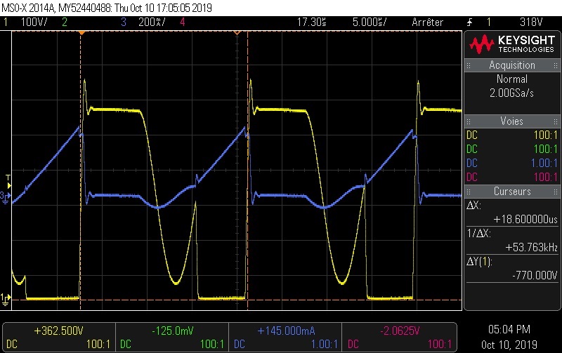
- The mosfet turn-off time. It opens approximatively in 400ns whereas it is given for a turn-off time of 24ns (gate/ source charge = 10nC). So, it is not fast enough to make the zener clamp active. There is only 10Ω on the gate...
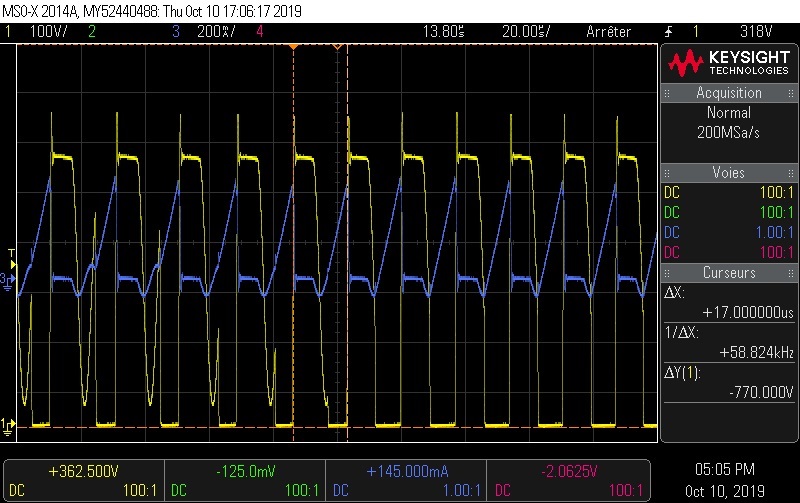
- The frequency: our switching frequency is quite low as well, it varies around 60kHz, when we should actually be around 80kHz. 


Despite these points, the power supply works quite well, the output voltage is stable (200mV ripple) at the desired load.


How can we gain the missing 20% of efficiency ?

Thanks a lot for your help.

Best Regards.

Nicolas.


  • Hello Nicolas,

    Thank you for your interest In the UCC28730-Q1 PSR flyback controller. 

    I agree that you should be getting much higher efficiency than 55%.  The extra loss means that you have parasitic loads that are not accounted for.  Quite likely your snubbers may be oversized, and/or several other possibilities. 

    However, it will help greatly to have more information about your design than what is presented in your original posting.  Can you please provide the input and output specifications, transformer primary inductance, leakage inductance, and turns ratios, and a schematic drawing of your flyback converter?  Also, a waveform or two of the MOSFET switching behavior showing Vds, Vgs, and Ids if possible, plus the line and load conditions at which the waveforms were acquired.  Timebase sweeps to see one or two switching cycles and to see dozens of cycles.  This will help us diagnose the problem.

    Regards,
    Ulrich

  • Hi Ulrich,

    Thanks for your quick answer.

    You will find here below two screenshots of the Vds voltage and the primary current with two different timebases.

    We are unable to show you the Vgs signal, because either when we try to put a probe or a differential probe on the Vgs, the power supply does not work anymore. It seems that the probe disturbs the gate command.

    About specifications:

    - Input: 200Vrms @ 400Hz

    - Output: 38V @ 450mA (resistive load)

    - Transformer : 3844µH, Np/Na=9.69, Np/Ns=6.74

    We are fine with sending you the schematics, but not through the forum. May we send it through email ?

    Thanks for your help Ulrich.

    Regards.

    Nicolas.


  • Hello Nicolas,

    Thank you for the additional information.  I will ponder these screen shots while waiting for the schematic file (hopefully a pdf).  Please email to Ulrich_goerke@ti.com thanks. 

    Regards,
    Ulrich

  • Hello Nicolas,

    As we found through off-line email correspondence, the main problem with your apparently low efficiency was a calculation error.  In this case, Pout was correctly measured as Vout*Iout, but Pin was measured as Vin(rms) * Iin(rms), neglecting the power factor term PF.  When including the PF term (about 0.6~0.65), the calculated efficiency increased to the expected value.  This accounts for why the apparent extra-high loss did not result in any significant temperature rise of components.

    To answer the other questions:  the MOSFET's turn-off time of 24ns is specified with Id = 5A as a test condition.  In your design, peak drain current is a few hundred milliamps, so it takes ~400ns to charge up the non-linear Coss of that MOSFET. 

    This extra apparent on-time (from 400ns capacitive turn-off delay) allows the peak current to rise higher than expected.  The higher energy per cycle (1/2*Lm*Ipk^2) in turn results in a lower switching frequency needed to achieve regulation.   

    I believe this closes out this thread.

    Regards,
    Ulrich