This thread has been locked.

If you have a related question, please click the "Ask a related question" button in the top right corner. The newly created question will be automatically linked to this question.

LM5116: does not work as expected

Part Number: LM5116

The design is almost the same as if you fill in the 30-70V input, 24V 20A output at WEBENCH® Power Designer.

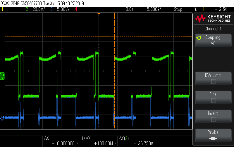
But the actual result is quite far from expected and there are some main problems, output voltage is 24V

1. LM5116 broke down easily, it broke at these situation: 70V input 10A output, broke down immediately; 48V input 13A output, broke down immediately

2. Temperature is quite high, when 60V input 10A output, the temperature rise to 100 degree in 3 minutes.

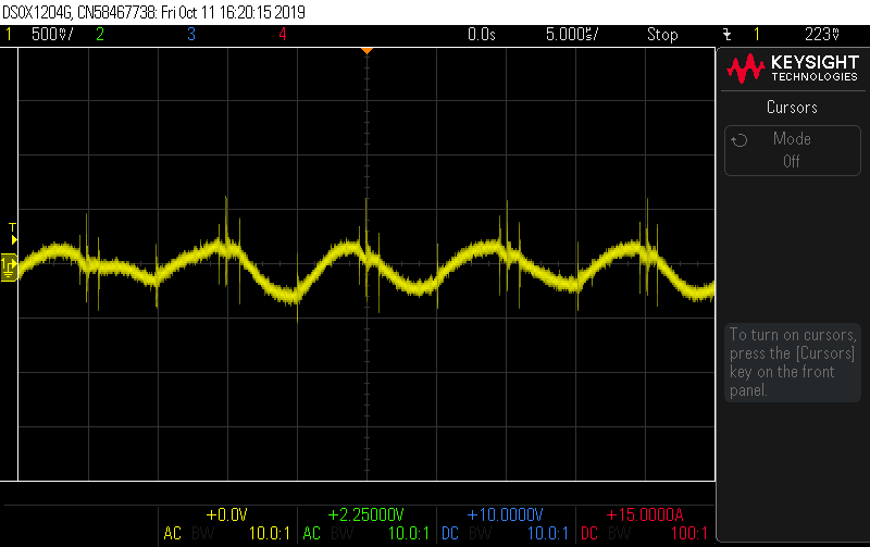
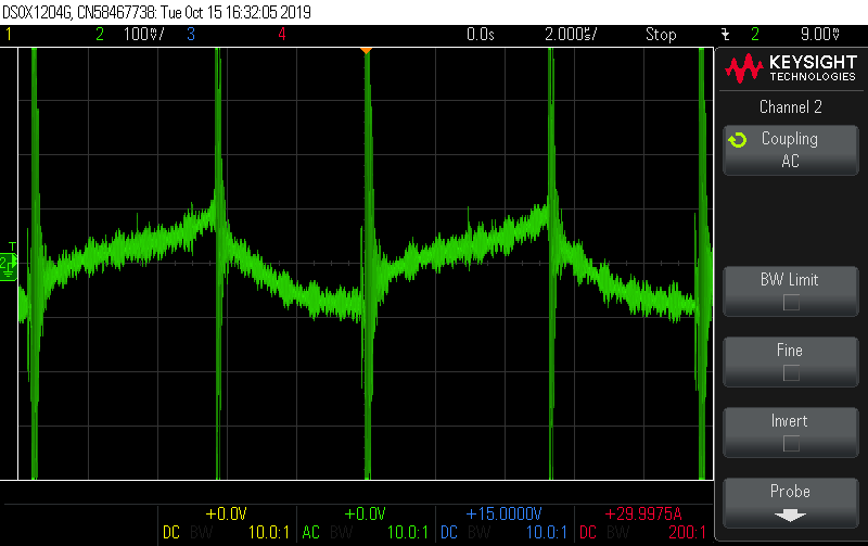
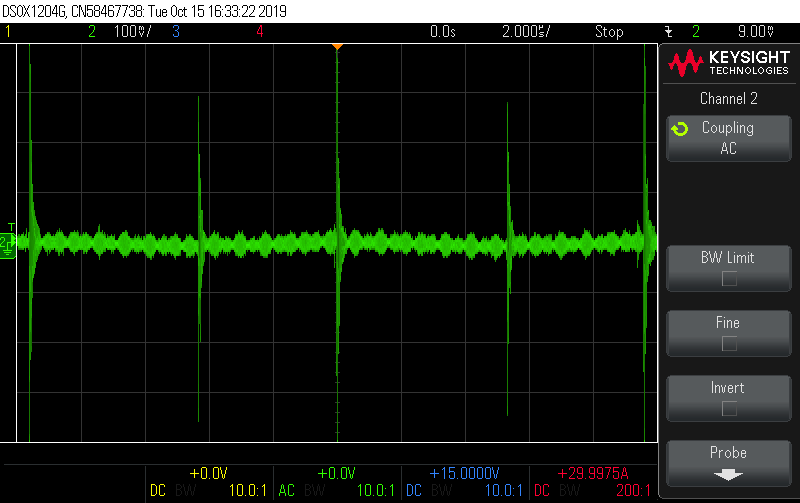
3. Large output ripple, it was about 1Vpp, and voltage spike when MOSFET on and off.

Is there any way to address these issues? Thank a lot!

 1185.lm5116.pdf

  • Hoi Keung Tang,

    Thank you for sharing the schematic, layout, and waveform as well as description of the issue. It looks like the issue lies in the layout.

    1. The best way to find root cause of a damaged IC is to probe different pins to see if the circuit is exceeding any absolute max ratings. Here are a few layout considerations which may be contributing to the possible EOS event. The IC may be breaking because there is no VIN capacitor close to the VIN pin of the IC. C4 should be placed close to the IC with a very small loop (VIN to cap+ to cap- to PGND) to provide a low-impedance source of high-frequency current. There is also a large loop in the power stage (CIN+ to Q1/2 to Z3/4 through R1 back to CIN-). It also appears that the SW node connects to large planes on midlayer 2 and the bottom layer close to the signal traces. This noisy node can corrupt the sensitive signals.

    2. The temperature of the IC will be higher than normal because the layout does not provide adequate heat sinking. The LM5116 has a thermal pad (exposed pad "EP") on the bottom of the IC. Your layout connects this to a small rectangle of copper on the top layer, then has thermal vias to mid-layer 1 which has lots of copper. The layout should have a large copper area on the top layer to get the most heat out, then rely on other layers to provide additional heatsinking. There is lots of underutilized copper on the top layer under P2 and around the bottom part of the board. This can be used for GND heatsinking if the VIN trace is moved to a mid-layer and C9/R7 are moved.

    3. It looks like the SW node has a long pulse, then short pulse, then long pulse, then short pulse. This is probably due to the coupled noise in the layout from the large SW area on mid-layer 2 and the bottom layer.

    -Sam

  • You can find more layout guidelines in the datasheet Layout Guidelines section.

  • Thanks for the reply.

    Will it be better if change the PCB from FR4 4 layer to aluminum 2 layer and pour all the cooper to GND? How about the MOSFET heat

    If I want to keep in FR4, how to pour the copper for better heat distribution? Will it be safe to run in 70Vinput, 24V 20A output? Because making FR4 will be much faster than aluminum and less weight.

    And how about the voltage ripple? It is much higher than expected.

    Any problem on the schematic, I tried to use the quick start calculator, it showed problem on boost trip capacitor.

    Thank a lot!

    4214.LM5116_quickstart.xls

  • Hoi Keung Tang,

    FR4 4-layer will work. You do not need to change the board material.

    The heat will spread the best through paths of low thermal conductivity. Try to have large copper pours on the board with a close direct connection to the hot component. Top layer is best because it does not require the heat to flow through the thin vias.

    Check the switch node. I think you may have an unsteady duty cycle. This is probably due to the SW coupling on mid-layer 2 and the bottom layer. You can test this by cutting the feedback trace and routing the VOUT connection directly to the feedback divider away from noisy nodes.

    The schematic looks good but you are right, the FETs may have too much capacitance. This would cause more heat dissipation in the IC (driving too much current) and more heat in the FETs (slower turn on/off SW loss). I will check with the team to confirm WEBENCH's recommendation.

    -Sam

  • With the original design, the  high side and 1 low side mosfet did not switch as expected. Then I removed 1 high side and 1 low side mosfet, changed the bootstrap capacitor to 4 0.1uF capacitor, and changed the switching frequency to 100khz. Now the voltage ripple and heat reduce to a acceptable level.

    I think the voltage ripple and be further reduce by increasing inductance and use a low ESR capacitor. But how to due with the voltage spike? I tried adding a resistor in high side and low side MOSFET, used a snubber circuit across low side MOSFET. Both did not work.

    And one more new question, when I tried to change the 270uF capacitor to 4 47uF capacitor, the high side MOSFET broken immediately, why is that?

    Original switching waveform with 5A load

    voltage spike with 10A load

  • Hoi Keung Tang,

    The output ripple will be greatly reduced by using low-ESR output capacitors.

    The voltage spike on the last waveform may be due to noise coupling through the scope from the SW node. Try measuring again without connecting the SW node to channel 3.

    VIN also appears to be oscillating. This can also cause issues with the proper operation of the controller. Try adding another 2.2uF capacitor on top of C5. If that does not work, try adding an electrolytic cap to dampen the oscillation.

    I'm not sure why changing COUT to ceramics caused the high-side FET to break. You can test again and check that you are not exceeding abs max for the FET or check that the temperature is not running away.

    -Sam

  • I added 4 100uF e-cap at the input, 2 in series then 2 parallel to get 100uF input capacitor, the input oscillation is gone, but these capacitors are very hot.

    The voltage spike seems real, I can pick up these spike using a probe near the PCB.

    One more new problem, the switching reduce half in high load now, why is that? below 5A load, it is fine, but above 5A, the switching frequency reduce half

    voltage spike

    probe pick up

  • And it seems that LM5116 broken easily, I am not sure it is due to input oscillation or not.

  • Hoi Keung Tang,

    The capacitors are very hot because there is large AC current passing through them due to the instability of the LM5116. The instability is probably coming from coupled noise from the large SW planes next to the sensitive traces.

    The voltage spike is a function of the ringing on SW and the parasitic capacitance of the inductor as well as the low-impedance path from VOUT back to GND for the high-frequency current. Your switch nodes looked okay from your scope shot so the issue is probably that there's no small ceramic capacitor connecting VOUT back to GND.

    The SW had large pulse, small pulse, large pulse, small pulse. If the small pulse gets any smaller, it may disappear completely which would explain the frequency reducing in half. This is due to the instability of the LM5116.

    The board will probably need to have a new layout. Follow the guidelines in the datasheet for guidance. And make sure you place a capacitor very close to the IC as well.

    -Sam

  • I do not think this PCB is that bad causing such many problems. I tried to seperate the IC and MOSFET using 2 PCB, 1 was just LM5116, 1 was MOSFET and inductor. Same problem occured.

    So far I think there are two problems using WEBENCH: bootstrap capacitor never change, it is always 0.1uF; the PCB files WEBENCH generated can not be used, footprint was wrong for some components and the board was seriously short circuit.WBDesign4_AltiumDesigner.zip

  • Hoi Keung Tang,

    The PCB does not have many problems. It's mostly just that the board needs a capacitor for the VIN of the IC and the board needs to reduce the area of the SW node especially around sensitive traces. The lack of capacitor can explain the damage to the IC and the SW node can explain the instability which explains the excessive input and output ripple. The layout can also have better thermal layout which explains the hot IC.

    You are correct, the WEBENCH design should recommend 1uF as stated in the datasheet to be more conservative. You can probe HB to see if the bootstrap voltage is collapsing. If so, increase the boot cap to 1uF.

    And the layout you've attached does have serious shorts. I will investigate this and make sure WEBENCH does not export a file like this.

    -Sam

  • Hoi Keung Tang,

    I've confirmed the layout issue and I've connected with the WEBENCH team to fix this.

    My WEBENCH designs all gave me 1uF for CBOOT. Can you please give me the inputs you used to get 0.1uF?

    Thanks,

    -Sam